AD9801 View Datasheet(PDF) - Analog Devices
Part Name
Description
Manufacturer
AD9801 Datasheet PDF : 12 Pages
| |||
AD9801
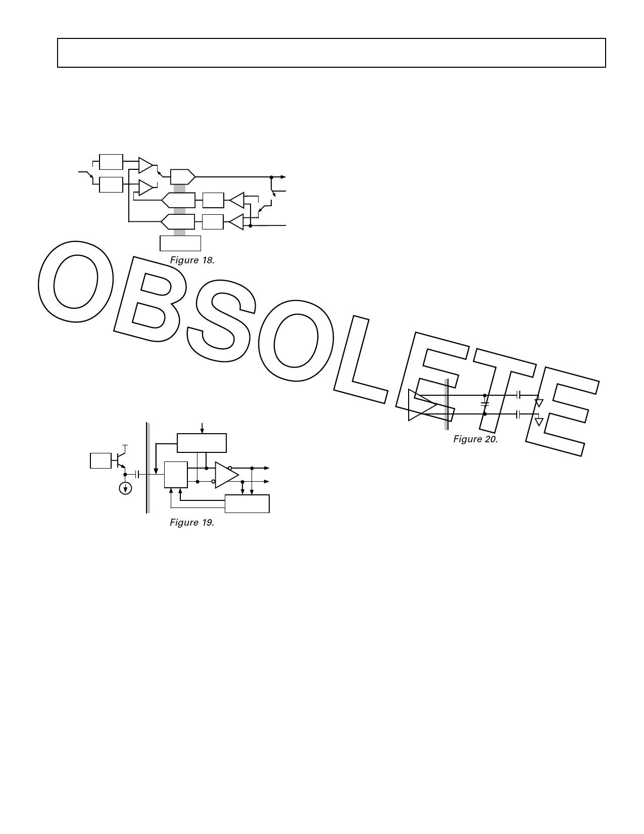
The actual implementation of this loop is slightly more compli-
cated as shown in Figure 18. Because there are two separate
CDS blocks, two black level feedback loops are required and
two offset voltages are developed. Figure 18 also shows an
additional PGA block in the feedback loop labeled “RPGA.”
To avoid problems associated with processing these transients,
the AD9801 includes an input blanking function. When active
(PBLK = LOW), this function stops the CDS operation and
allows the user to disconnect the CDS inputs from the CCD
buffer.
If the input voltage exceeds the supply rail by more than
CDS1
IN
CDS1
PGA
ADC
CLPOB
0.3 V, protection diodes will be turned on, increasing current
flow into the AD9801 (see Equivalent Input Circuits). Such
voltage levels should be externally clamped to prevent device
damage or reliability degradation.
RPGA2 INT2
10-Bit Analog-to-Digital Converter (ADC)
The ADC employs a multibit pipelined architecture, which is
RPGA1 INT1
NEG REF
well-suited for high throughput rates while being both area and
OBSOLETE CONTROL
Figure 18.
The RPGA uses the same control inputs as the PGA, but has
the inverse gain. The RPGA functions to attenuate by the same
factor as the PGA amplifies, keeping the gain and bandwidth of
the loop constant.
Input Bias Level Clamping
The buffered CCD output is connected to the AD9801 through
an external coupling capacitor. The dc bias point for this coupling
capacitor is established during the clamping (CLPDM = LOW)
period using the “dummy clamp” loop shown in Figure 19.
When closed around the CDS, this loop establishes the desired
DC bias point on the coupling capacitor.
CLPDM
power efficient. The multistep pipeline presents a low input
capacitance resulting in lower on-chip drive requirements. A
fully differential implementation was used to overcome head-
room constraints of the single +3 V power supply.
Differential Reference
The AD9801 includes a 0.5 V reference based on a differential,
continuous-time bandgap cell. Use of an external bypass
capacitor reduces the reference drive requirements, thus
lowering the power dissipation. The differential architecture was
chosen for its ability to reject supply and substrate noise.
Recommended decoupling shown in Figure 20.
REF
VRT
VRB
0.1µF
1µF
0.1µF
INPUT
Figure 20.
CLAMP
Internal Timing
CCD
The AD9801’s on-chip timing circuitry generates all clocks
CDS
PGA
TO ADC
necessary for operation of the CDS and ADC blocks. The user
needs only to synchronize the SHP and SHD clocks with the
Figure 19.
BLACK
LEVEL CLP
CCD waveform, as all other timing is handled internally. The
ADCCLK signal is used to strobe the output data, and can be
adjusted to accommodate desired timing.
Input Blanking
In some applications, the AD9801’s input may be exposed to
large signals from the CCD. These signals can be very large,
relative to the AD9801’s input range, and could thus saturate
on-chip circuit blocks. Recovery time from such saturation
conditions could be substantial.
REV. 0
–9–
Share Link: 