ADM1021A(2012) View Datasheet(PDF) - ON Semiconductor
Part Name
Description
Manufacturer
ADM1021A Datasheet PDF : 16 Pages
| |||
ADM1021A
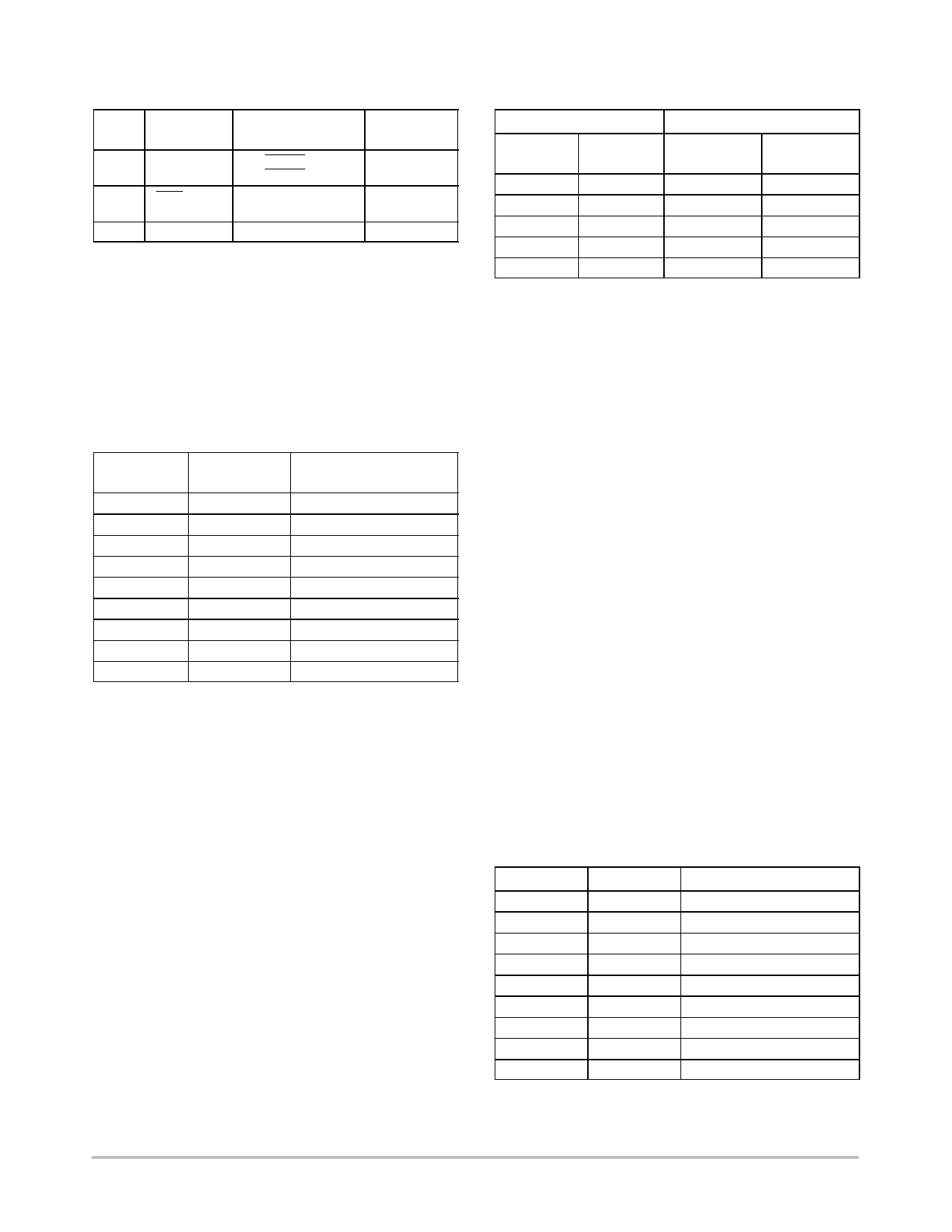
Table 8. CONFIGURATION REGISTER BIT
ASSIGNMENTS
Bit
7
6
5 to 0
Name
MASK1
RUN/STOP
Function
0 = ALERT Enabled
1 = ALERT Masked
0 = Run
1 = Standby
Reserved
Power-on
Default
0
0
0
Conversion Rate Register
The lowest three bits of this register are used to program
the conversion rate by dividing the ADC clock by 1, 2, 4, 8,
16, 32, 64, or 128 to give conversion times from 125 ms
(Code 0x07) to 16 seconds (Code 0x00). This register can be
written to and read back over the SMBus. The higher five
bits of this register are unused and must be set to 0. Use of
slower conversion times greatly reduces the device power
consumption, as shown in Table 9.
Table 9. CONVERSION RATE REGISTER CODE
Data
0x00
0x01
0x02
0x03
0x04
0x05
0x06
0x07
0x08 to 0xFF
Conversion/
Sec
0.0625
0.125
0.25
0.5
1
2
4
8
Reserved
Average Supply Current
mA Typ at VCC = 3.3 V
150
150
150
150
150
150
160
180
−
Limit Registers
The ADM1021A has four limit registers to store local and
remote and high and low temperature limits. These registers
can be written to and read back over the SMBus. The high
limit registers perform a > comparison, while the low limit
registers perform a < comparison. For example, if the high
limit register is programmed as a limit of 80C, measuring
81C results in an alarm condition. Even though the
temperature measurement range is from 0 to 127C, it is
possible to program the limit register with negative values.
This is for backwards compatibility with the ADM1021.
Offset Register
An offset register is provided at Address 0x11. This
allows the user to remove errors from the measured remote
temperature. These errors can be introduced by clock noise
and PCB track resistance. See Table 10 for an example of
offset values.
The offset value is stored as an 8-bit, twos complement
value. The value of the offset is negative if the MSB of
Register 0x11 is 1, and is positive if the MSB of
Register 0x11 is 0. This value is added to the remote
temperature. The offset register defaults to 0 at powerup.
The offset register range is −128C to +127C.
Table 10. OFFSET VALUES
Offset Register
(0x11)
1111 1100
1111 1111
0000 0000
0000 0001
0000 0100
Offset
Value
−4C
−1C
0C
+1C
+4C
Remote Temperature
(With
Offset)
(Without
Offset)
14C
18C
17C
18C
18C
18C
19C
22C
18C
18C
One-shot Register
The one-shot register is used to initiate a single conversion
and comparison cycle when the ADM1021A is in standby
mode, after which the device returns to standby. This is not
a data register as such, and it is the write operation that
causes the one-shot conversion. The data written to this
address is irrelevant and is not stored.
Serial Bus Interface
Control of the ADM1021A is carried out via the serial bus.
The ADM1021A is connected to this bus as a slave device,
under the control of a master device. Note that the SMBus
and SCL pins are three-stated when the ADM1021A is
powered down and will not pull down the SMBus.
Address Pins
In general, every SMBus device has a 7-bit device address
(except for some devices that have extended 10-bit
addresses). When the master device sends a device address
over the bus, the slave device with that address responds.
The ADM1021A has two address pins, ADD0 and ADD1,
to allow selection of the device address so that several
ADM1021A’s can be used on the same bus, and/or to avoid
conflict with other devices. Although only two address pins
are provided, these are three-state and can be grounded, left
unconnected, or tied to VDD so that a total of nine different
addresses are possible, as shown in Table 11.
It should be noted that the state of the address pins is only
sampled at powerup, so changing them after powerup has no
effect.
http://onsemi.com
10
Share Link: 