ADM1021A(2012) View Datasheet(PDF) - ON Semiconductor
Part Name
Description
Manufacturer
ADM1021A Datasheet PDF : 16 Pages
| |||
ADM1021A
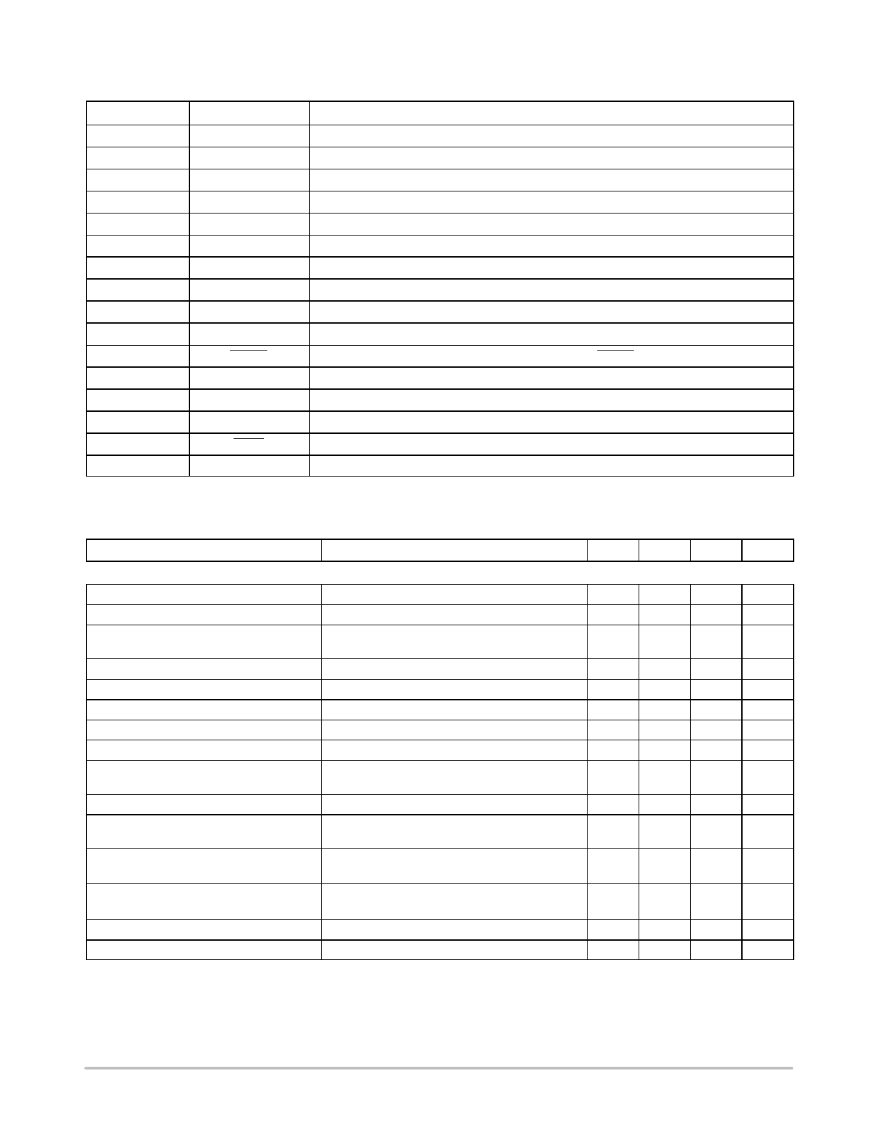
Table 2. ABSOLUTE MAXIMUM RATINGS
Parameter
Rating
Unit
Positive Supply Voltage (VDD) to GND
D+, ADD0, ADD1
D− to GND
−0.3 to +6.0
V
−0.3 to VDD + 0.3
V
−0.3 to +0.6
SCLK, SDATA, ALERT, STBY
Input Current
Input Current, D−
−0.3 to +6.0
V
50
mA
1
mA
ESD Rating, All Pins (Human Body Model)
2,000
V
Continuous Power Dissipation
Up to 70C
Derating Above 70C
650
mW
6.7
mW/C
Operating Temperature Range
−55 to +125
C
Maximum Junction Temperature (TJ MAX)
Storage Temperature Range
150
C
−65 to +150
C
Lead Temperature, Soldering (10 sec)
300
C
IR Reflow Peak Temperature
220
C
Stresses exceeding Maximum Ratings may damage the device. Maximum Ratings are stress ratings only. Functional operation above the
Recommended Operating Conditions is not implied. Extended exposure to stresses above the Recommended Operating Conditions may affect
device reliability.
NOTE: This device is ESD sensitive. Use standard ESD precautions when handling.
Table 3. THERMAL CHARACTERISTICS
Package Type
16-lead QSOP Package
qJA
Unit
105
C/W
Table 4. ELECTRICAL CHARACTERISTICS
(TA = TMIN to TMAX, VDD = 3.0 V to 3.6 V, unless otherwise noted) (Note 1)
Parameter
Test Conditions/Comments
Power Supply and ADC
Temperature Resolution
Guaranteed No Missed Codes
Temperature Error, Local Sensor
Temperature Error, Remote Sensor
TA = 60C to 100C
Supply Voltage Range (Note 2)
Undervoltage Lockout Threshold
Undervoltage Lockout Hysteresis
Power-On Reset Threshold
POR Threshold Hysteresis
Standby Supply Current
Average Operating Supply Current
Auto−convert Mode, Averaged Over 4 Sec
Conversion Time
Remote Sensor Source Current
D− Source Voltage
Address Pin Bias Current (ADD0, ADD1)
VDD Input, Disables ADC, Rising Edge
VDD, falling edge (Note 3)
VDD = 3.3 V, No SMBus Activity
SCLK at 10 kHz
0.25 Conversions/Sec Rate
2 Conversions/Sec Rate
From Stop Bit to Conversion Complete
(Both Channels) D+ Forced to D− + 0.65 V
High Level (Note 3)
Low Level (Note 3)
Momentary at Power-on Reset
Min
Typ
Max Unit
1.0
−
−
C
−3.0
1.0
+3.0
C
−3.0
−
+3.0
C
−5.0
−
+5.0
3.0
−
3.6
V
2.5
2.7
2.95
V
−
25
−
mV
0.9
1.7
2.2
V
−
50
−
mV
−
1.0
5.0
mA
−
4.0
−
−
130
200
mA
−
225
370
mA
65
115
170
ms
120
205
300
mA
7.0
12
16
−
0.7
−
V
−
50
−
mA
http://onsemi.com
3
Share Link: 