ADM1021AARQZ-R View Datasheet(PDF) - ON Semiconductor
Part Name
Description
Manufacturer
ADM1021AARQZ-R Datasheet PDF : 15 Pages
| |||
ADM1021A
ELECTRICAL CHARACTERISTICS (TA = TMIN to TMAX, VDD = 3.0 V to 3.6 V, unless otherwise noted. (Note 1)
Parameter
Test Conditions / Comments
Min
Typ
Max
Unit
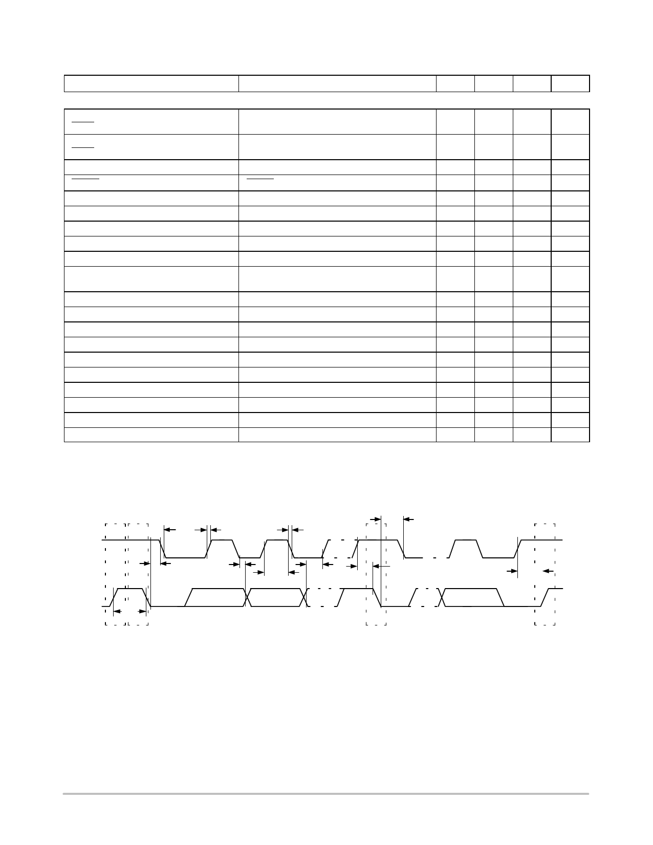
SMBus Interface (See Figure 2)
Logic Input High Voltage, VIH
STBY, SCLK, SDATA
VDD = 3.0 V to 5.5 V
2.2
V
Logic Input Low Voltage, VIL
STBY, SCLK, SDATA
VDD = 3.0 V to 5.5 V
0.8
V
SMBus Output Low Sink Current
SDATA forced to 0.6 V
6.0
mA
ALERT Output Low Sink Current
ALERT forced to 0.4 V
1.0
mA
Logic Input Current, IIH, IIL
SMBus Input Capacitance, SCLK, SDATA
−1.0
+1.0
mA
5.0
pF
SMBus Clock Frequency
100
kHz
SMBus Clock Low Time, tLOW
tLOW between 10% points
4.7
ms
SMBus Clock High Time, tHIGH
tHIGH between 90% points
4.0
ms
SMBus Start Condition Setup Time,
tSU:STA
4.7
ms
SMBus Repeat Start Condition
250
ns
Setup Time, tSU:STA
Between 90% and 90% points
250
ns
SMBus Start Condition Hold Time, tHD:STA Time from 10% of SDATA to 90% of SCLK
4.0
ms
SMBus Stop Condition Setup Time, tSU:STO Time from 90% of SCLK to 10% of SDATA
4.0
ms
SMBus Data Valid to SCLK
Time for 10% or 90% of SDATA to 10% of SCLK
250
ns
Rising Edge Time, tSU:DAT
SMBus Data Hold Time, tBUF:DAT
SMBus Bus Free Time, tBUF
SCLK Falling Edge to SDATA
Time for 10% or 90% of SDATA to 10% of SCLK
250
0
Between start/stop condition
4.7
Valid Time, tVD:DAT
Master clocking in data
1. TMAX = 100°C, TMIN = 0°C
2. Operation at VDD = 5.0 V guaranteed by design; not production tested.
3. Guaranteed by design; not production tested.
ns
ms
ms
1
ms
1
ms
SCL
tLOW
tHD;STA
SDA
tBUF
P
S
tR
tHD;DAT
tF
tHIGH
tSU;DAT
tHD;STA
tSU;STA
S
Figure 2. Diagram for Serial Bus Timing
tSU;STO
P
http://onsemi.com
4
Share Link: 