ADP7102ACPZ-R7(RevA) View Datasheet(PDF) - Analog Devices
Part Name
Description
Manufacturer
ADP7102ACPZ-R7 Datasheet PDF : 28 Pages
| |||
Data Sheet
20 V, 300 mA, Low Noise, CMOS LDO
ADP7102
FEATURES
Input voltage range: 3.3 V to 20 V
Maximum output current: 300 mA
Low noise: 15 µV rms for fixed output versions
PSRR performance of 60 dB at 10 kHz, VOUT = 3.3 V
Reverse current protection
Low dropout voltage: 200 mV at 300 mA load
Initial accuracy: ±0.8%
Accuracy over line, load, and temperature: −2%, +1%
Low quiescent current (VIN = 5 V), IGND = 750 μA with 300 mA
load
Low shutdown current: 40 µA at VIN = 12 V
Stable with small 1 µF ceramic output capacitor
7 fixed output voltage options: 1.5 V, 1.8 V, 2.5 V, 3 V, 3.3 V,
5 V, and 9 V
Adjustable output from 1.22 V to VIN – VDO
Foldback current limit and thermal overload protection
User programmable precision UVLO/enable
Power good indicator
8-lead LFCSP and 8-lead SOIC packages
APPLICATIONS
Regulation to noise sensitive applications: ADC, DAC
circuits, precision amplifiers, high frequency oscillators,
clocks, and PLLs
Communications and infrastructure
Medical and healthcare
Industrial and instrumentation
GENERAL DESCRIPTION
The ADP7102 is a CMOS, low dropout linear regulator that
operates from 3.3 V to 20 V and provides up to 300 mA of
output current. This high input voltage LDO is ideal for
regulation of high performance analog and mixed signal
circuits operating from 19 V to 1.22 V rails. Using an
advanced proprietary architecture, it provides high power
supply rejection, low noise, and achieves excellent line and
load transient response with just a small 1 µF ceramic
output capacitor.
The ADP7102 is available in 7 fixed output voltage options and
an adjustable version, which allows output voltages that range
from 1.22 V to VIN − VDO via an external feedback divider.
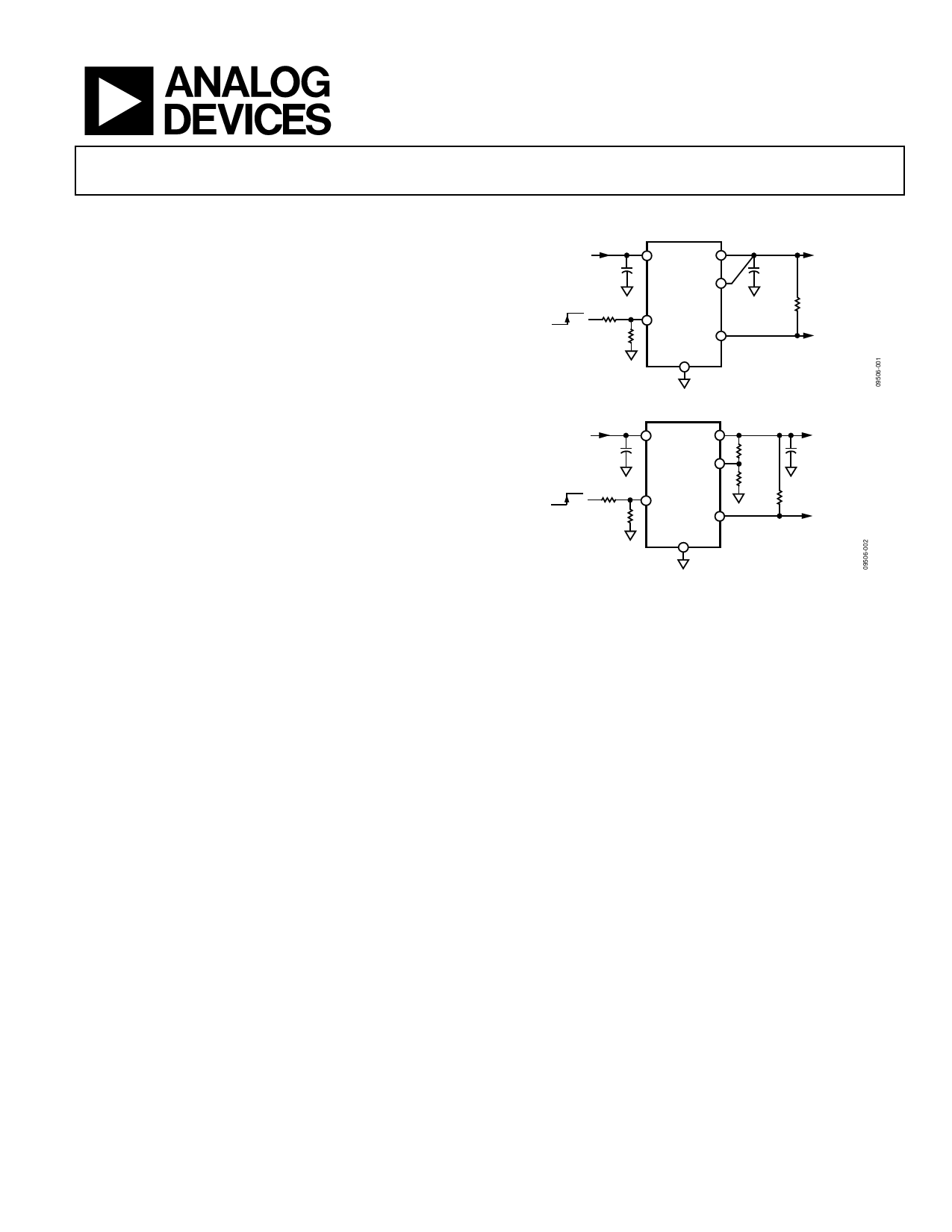
TYPICAL APPLICATION CIRCUITS
VIN = 8V
CIN +
1µF
OFF
ON
R1
100kΩ
R2
100kΩ
VIN VOUT
SENSE
EN/
UVLO
PG
GND
+ COUT
1µF
VOUT = 5V
RPG
100kΩ
PG
Figure 1. ADP7102 with Fixed Output Voltage, 5 V
VIN = 8V
CIN +
1µF
ON
OFF
R3
100kΩ
R4
100kΩ
VIN VOUT
ADJ
EN/
UVLO
PG
GND
R1
40.2kΩ
VOUT = 5V
+ COUT
1µF
R2
13kΩ
RPG
100kΩ
PG
Figure 2. ADP7102 with Adjustable Output Voltage, 5 V
The ADP7102 output noise voltage is 15 μV rms and is inde-
pendent of the output voltage. A digital power good output
allows power system monitors to check the health of the output
voltage. A user programmable precision undervoltage lockout
function facilitates sequencing of multiple power supplies.
The ADP7102 is available in 8-lead, 3 mm × 3 mm LFCSP
and 8-lead SOIC packages. The LFCSP offers a very compact
solution and also provides excellent thermal performance for
applications requiring up to 300 mA of output current in a
small, low-profile footprint.
Rev. A
Information furnished by Analog Devices is believed to be accurate and reliable. However, no
responsibility is assumed by Analog Devices for its use, nor for any infringements of patents or other
rights of third parties that may result from its use. Specifications subject to change without notice. No
license is granted by implication or otherwise under any patent or patent rights of Analog Devices.
Trademarks and registered trademarks are the property of their respective owners.
One Technology Way, P.O. Box 9106, Norwood, MA 02062-9106, U.S.A.
Tel: 781.329.4700
www.analog.com
Fax: 781.461.3113
©2011 Analog Devices, Inc. All rights reserved.
Share Link: 