ADV7123JSTZ240 View Datasheet(PDF) - Analog Devices
Part Name
Description
Manufacturer
ADV7123JSTZ240 Datasheet PDF : 24 Pages
| |||
ADV7123
3.3 V TIMING SPECIFICATIONS
VAA = 3.0 V to 3.6 V,1 VREF = 1.235 V, RSET = 560 Ω, CL = 10 pF. All specifications TMIN to TMAX,2 unless otherwise noted, TJ MAX = 110°C.
Table 6.
Parameter3
ANALOG OUTPUTS
Analog Output Delay
Analog Output Rise/Fall Time4
Analog Output Transition Time5
Analog Output Skew6
CLOCK CONTROL
CLOCK Frequency7
Data and Control Setup
Data and Control Hold
CLOCK Period
CLOCK Pulse Width High6
CLOCK Pulse Width Low6
CLOCK Pulse Width High
CLOCK Pulse Width Low
CLOCK Pulse Width High
CLOCK Pulse Width Low
CLOCK Pulse Width High
CLOCK Pulse Width Low
Pipeline Delay6
PSAVE Up Time6
Symbol
t6
t7
t8
t9
fCLK
t1
t2
t3
t4
t5
t4
t5
t4
t5
t4
t5
tPD
t10
Min
Typ Max Unit
7.5
ns
1.0
ns
15
ns
12
ns
50
MHz
140 MHz
240 MHz
330 MHz
0.2
ns
1.5
ns
3
ns
1.4
ns
1.4
ns
1.875
ns
1.875
ns
2.85
ns
2.85
ns
8.0
ns
8.0
ns
1.0
1.0 1.0
Clock cycles
4
10
ns
Conditions
50 MHz grade
140 MHz grade
240 MHz grade
330 MHz grade
fCLK_MAX = 330 MHz
fCLK_MAX = 330 MHz
fCLK_MAX = 240 MHz
fCLK_MAX = 240 MHz
fCLK_MAX = 140 MHz
fCLK_MAX = 140 MHz
fCLK_MAX = 50 MHz
fCLK_MAX = 50 MHz
1 These maximum and minimum specifications are guaranteed over this range.
2 Temperature range: TMIN to TMAX: −40°C to +85°C at 50 MHz and 140 MHz, 0°C to 70°C at 240 MHz and 330 MHz.
3 Timing specifications are measured with input levels of 3.0 V (VIH) and 0 V (VIL) 0 for both 5 V and 3.3 V supplies.
4 Rise time was measured from the 10% to 90% point of zero to full-scale transition, fall time from the 90% to 10% point of a full-scale transition.
5 Measured from 50% point of full-scale transition to 2% of final value.
6 Guaranteed by characterization.
7 fCLK maximum specification production tested at 125 MHz; 5 V limits specified here are guaranteed by characterization.
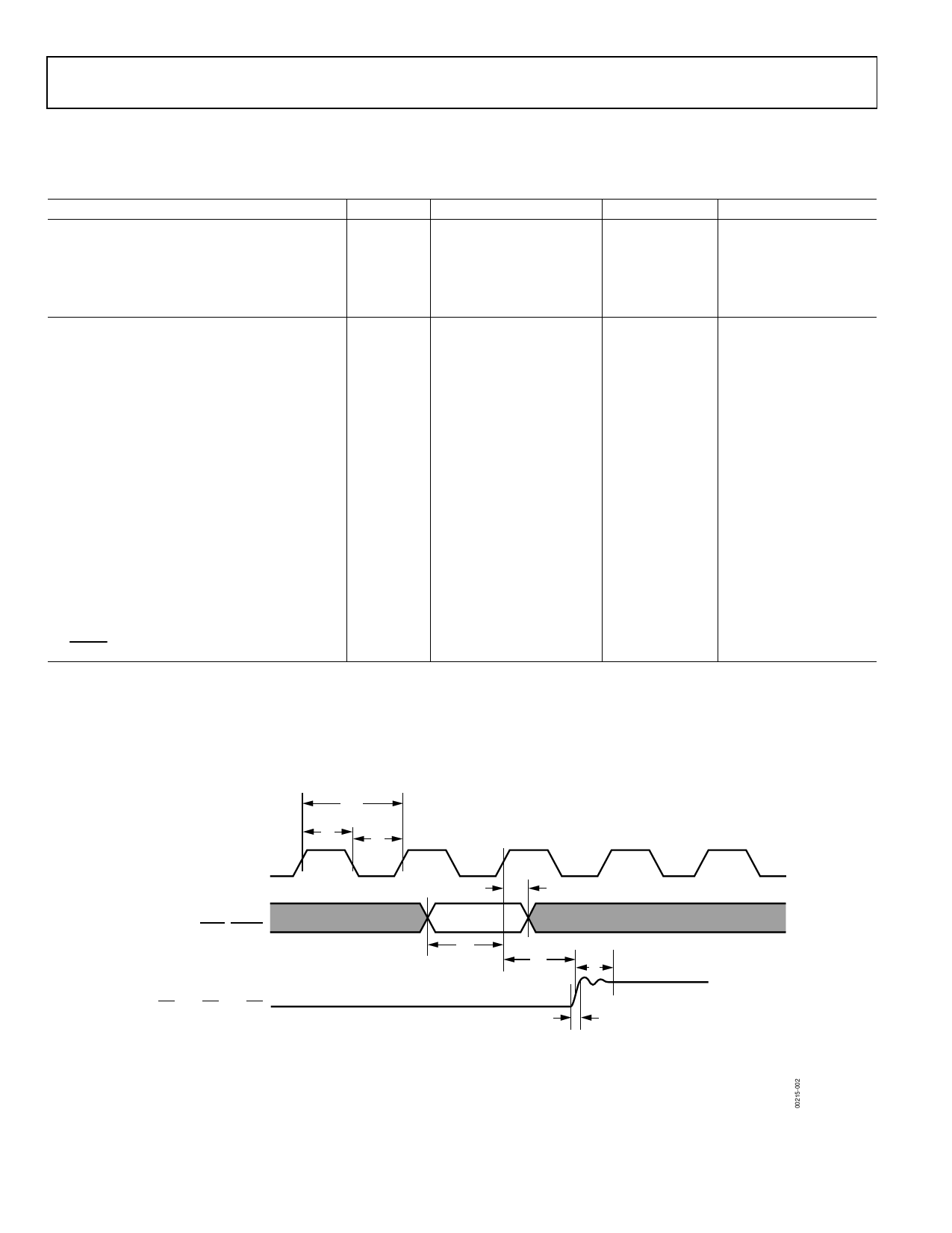
t3
t4
t5
CLOCK
DIGITAL INPUTS
(R9 TO R0, G9 TO G0, B9 TO B0,
SYNC, BLANK)
t2
t1
t6
t8
ANALOG OUTPUTS
(IOR, IOR, IOG, IOG, IOB, IOB)
t7
NOTES
1. OUTPUT DELAY (t6) MEASURED FROM THE 50% POINT OF THE RISING EDGE OF CLOCK TO THE 50% POINT
OF FULL-SCALE TRANSITION.
2. OUTPUT RISE/FALL TIME (t7) MEASURED BETWEEN THE 10% AND 90% POINTS OF FULL-SCALE TRANSITION.
3. TRANSITION TIME (t8) MEASURED FROM THE 50% POINT OF FULL-SCALE TRANSITION TO WITHIN 2% OF THE
FINAL OUTPUT VALUE.
Figure 2. Timing Diagram
Rev. D | Page 8 of 24
Share Link: 