APA3002 View Datasheet(PDF) - Anpec Electronics
Part Name
Description
Manufacturer
APA3002 Datasheet PDF : 29 Pages
| |||
APA3002
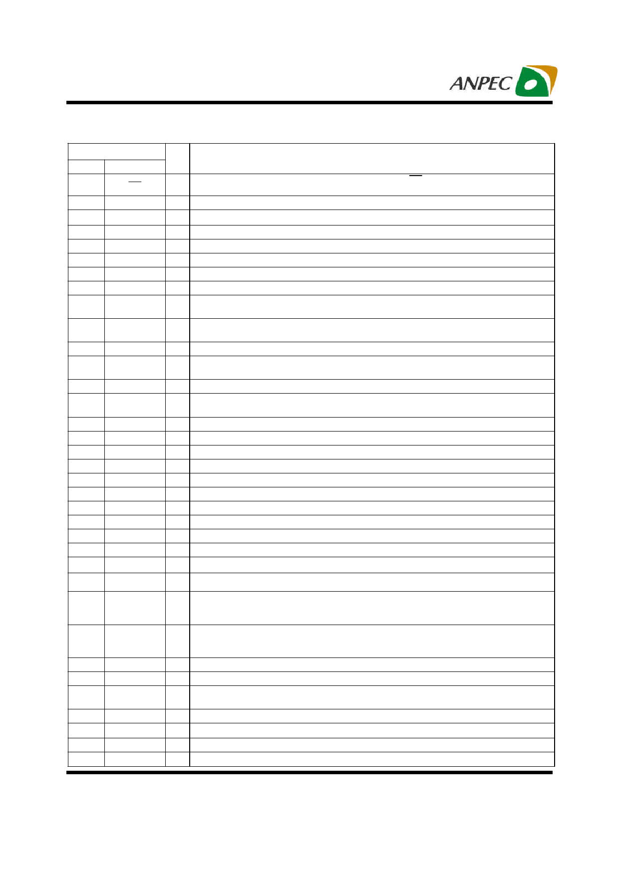
Pin Description
PIN
NO.
NAME
1
SD
2
RIN-
3
RIN+
4
2.5VREF
5
LIN+
6
LIN-
7
LDOREF
8
VREF
9
VARDIFF
10
VARMAX
11
VOLUME
12
REFGND
13
14,15,22
,23
16,17
18,19
20,21
24
25
26,30
27
28
29
31
32
LBS-
LPVDD
LOUT-
LPGND
LOUT+
LBS+
LCLAMP
AGND
ROSC
COSC
5VLDO
LVAROUT
RVAROUT
33
AVDD
34
MODE
35
MODEOUT
36
37
38,39,46
,47
40,41
42,43
44,45
48
RCLAMP
RBS+
RPVDD
ROUT+
RPGND
ROUT-
RBS-
I/O
FUNCTION
I Shutdown mode control signal input. Pulling the voltage on SD below 0.8V makes the IC enter
low-power shutdown mode with 10µA (typical) IDD.
I Right channel negative input.
I Right channel positive input.
O 2.5V reference for analog circuits.
I Left channel positive input.
I Left channel negative input.
O 5V reference output (5V LDO), connect it to VREF pin.
I Gain control section’s reference voltage input.
I
Input pin to set the difference in gain between the VAROUT and Class-D outputs by using the DC
voltage. Connect this pin to the ground or LDOREF when the VAROUT is not used.
I
Input pin to set the maximum gain of VAROUT by using the DC voltage. Connect this pin to
ground or LDOREF directly when the VAROUT is not used.
1 Input pin to set the gain of VAROUT and Class-D outputs by using the DC voltage.
-
Ground for gain control circuitry. Connect to AGND. If using a DAC to control the volume, connect
the DAC ground to this terminal.
I/O Left channel bootstrap power input for negative high-side MOSFET.
- Power supply for left channel H-bridge.
O Class-D left channel negative output.
- Power ground for left channel H-bridge.
O Class-D left channel positive output.
I/O Left channel bootstrap power input for positive high-side MOSFET.
- Left channel internal voltage supply output for bootstrap capacitor.
- Analog ground.
I/O Voltage of ROSC pin equal 0.125VDD, current setting resistor for internal ramp generator.
I/O Charge/Discharge capacitor for generating triangle wave.
O Internal 5V regulator output for external headphone driver used.
O Left channel variable audio output, for external headphone driver.
O Right channel variable audio output, for external headphone driver.
- Analog power supply (8.5 to 14V).
Control pin for amplifier operation. A logic high places the amplifier in variable output mode, and
I the Class-D output will disable; a logic low places the amplifier in variable output mode (line-level
output for external amplifier) and stereo Class-D outputs.
Inverse output of MODE pin, this pin can control the external headphone driver’s (APA4801) mute
O pin for changing operation from speaker operation to headphone operation. Leave this pin
unconnected when the external headphone driver is not in using.
- Right channel internal voltage supply output for bootstrap capacitor.
I/O Right channel bootstrap voltage input for positive high-side MOSFET.
- Power supply for right channel H-bridge.
O Class-D right channel positive output.
- Power ground for right channel H-bridge.
O Class-D right channel negative output.
I/O Right channel bootstrap voltage input for negative high-side MOSFET.
Copyright © ANPEC Electronics Corp.
13
Rev. A.6 - Sep., 2009
www.anpec.com.tw
Share Link: 