AS28F128J3M View Datasheet(PDF) - Austin Semiconductor
Part Name
Description
Manufacturer
AS28F128J3M Datasheet PDF : 8 Pages
| |||
Austin Semiconductor, Inc.
PEM
AS28F128J3M
Q-Flash
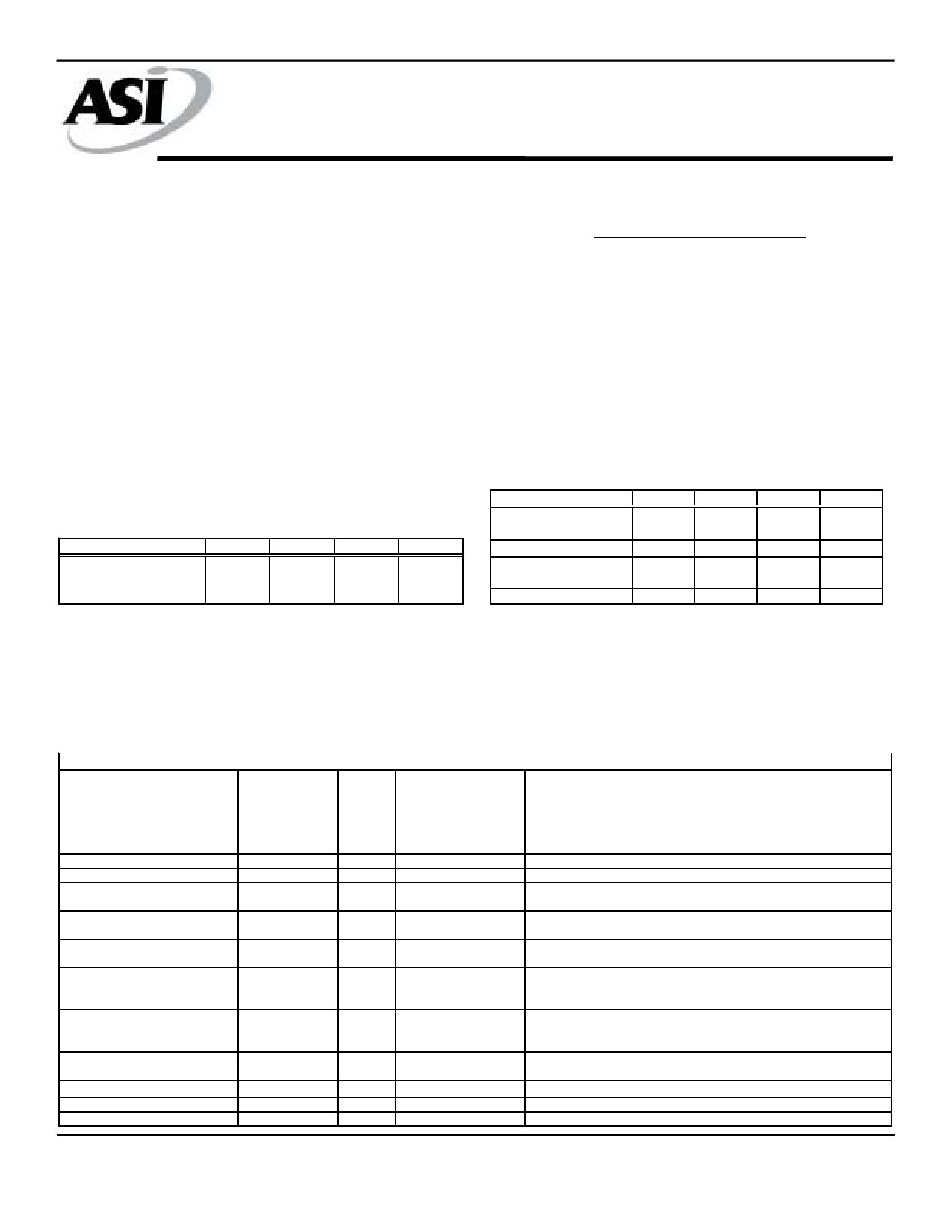
Three Chip Enable (CEx) pins are used for enabling and disabling Chip Enable Truth Table
the device by activating the device’s control logic, input buffer,
decoders, and sense amplifiers.
CE2 CE1
BYTE\ enables the device to be used in x8 or x16 configuration.
Byte=Low (logic 0) selects and 8-bit mode with address zero (A0)
selecting the High or Low Byte and Byte=High (logic 1) selects
the 16-bit or Word mode. When the device is in Word mode,
address one (A1) becomes the low order address bit and address
zero (A0) becomes a no-connect (NC).
VIL VIL
VIL VIL
VIL VIH
VIL VIH
VIH VIL
VIH VIL
VIH VIH
RP\ is used to reset the device. When the device is disabled and
VIH VIH
RP\ is at VCC, the STANDBY mode is enabled. A reset time
(tRWH) is required after RP\ switches to a High (logic 1) and the
outputs become valid. Likewise, the device has a wake time (tRS)
from RP\ High until WRITES to the Command User Interface
[CUI] are recognized, RESETS the ISM and clears the status Absolute Maximum Ratings
register.
Voltage
Min
Capacitance
Parameter/Condition Symbol
Typ
Input Capacitance
Cin
5
Output Capacitance Cbyte
14
Cout
5
Max
Units
8
pF
16
pF
12
pF
Temperature under
-55
Bias
Storage Temperature
-65
For VCCQ=2.7v to 3.6v -2
Voltage on any pin
Short Circuit Current
CE0
VIL
VIH
VIL
VIH
VIL
VIH
VIL
VIH
Max
125
125
5
100
Device
Enabled
Disabled
Disabled
Disabled
Enabled
Enabled
Enabled
Disabled
Units
0C
0C
V
mA
Notes
1
Stress greater than those listed under ABSOLUTE MAXIMUM RATINGS may
cause permanent damage to the device. This is a stress rating only and functional
operation of the device at these or any other conditions greater than those
indicated in the operational sections of this specification is not implied. Exposure
to absolute maximum conditions for any duration or segment of time may affect
device reliability.
Pin Description Table:
Notes
1: All specified voltages are with respect to GND. Minimum DC
voltage is -0.5v on input/output pins and -0.2v on Vcc and VPEN
pins. During transitions, this level may undershoot to -2.0v for
periods </= 20ns. Maximum DC voltage on input/output pins,
Vcc and VPEN is VCC+0.5V which, during transitions, may
overshoot to Vcc + 2.0v for periods <20ns.
Signal Name
Address
Chip Enables
Write Enable
Reset/Power-Down
Output Enable
Byte Mode Control
Programming Voltage
Status Pin/Flag
Input/Output Voltage
Supply Voltage
Digital Ground
No Connect(s)
AS28F128J3MRG
Revision 5.0 11/23/04
Symbol
Type
A0, A1, A2. A3, Input
A4, A5, A6, A7
A8, A9, A10, A11
A12,A13,A14,A15
A16,A17,A18,A19
A20,A21,A22,A23
CE0, CE1, CE2 Input
WE\
Input
RP\
Input
Pin
32,28,27,26,
25,24,23,22,
20,19,18,17,
13,12,11,10,
8,7,6,5,
4,3,1,30
14,2,29
55
16
OE\
Input
54
BYTE\
Input
31
VPEN
Input
15
STS
Output
53
VCCQ
VCC
GND
NC
Supply
Supply
Supply
-
43
9, 37
21, 42, 48
1, 30, 56
Description
Address Inputs during READ and WRITE Operations. A0 is only
used in x8 mode and will be a NC in x16 mode.
Three Chip Enable pins for Multiple devices. See chart for function
Write Control
Reset/Power-Down, When Low the control pin resets the status Reg.
and ISM to array READ mode.
Ouput Enable control enable data output buffers when Low, and when
High the output buffers are disabled
Configuration Control pin. When High the device is in x16 mode, when
Low the device is in Byte mode (x8)
Necessary Voltage pin for Programming, Erasing or configuring lock
bits. Typically connected to VCC. When VPEN</=VPENLK, this
enables Hardware Write Protect.
Indicates the status of the ISM. When configured in level mode, STS
acts as a RY/BY\ pin. When configured in its pulse mode, it can
pulse to indicate PROGRAM and or ERASE completion.
Separate/Isolated Voltage supply for Input/Output bus. Allows
voltage matching to different interface standards.
Power Supply: 2.7V - 3.6V
Ground
No electrical connection or function
Austin Semiconductor, Inc. reserves the right to change products or modify product specifications with appropriate notification
For Additional Products and Information visit out Web site at www.austinsemiconductor.com
3
Share Link: 