BTS725L1 View Datasheet(PDF) - Siemens AG
Part Name
Description
Manufacturer
BTS725L1 Datasheet PDF : 14 Pages
| |||
Preliminary BTS 725 L1
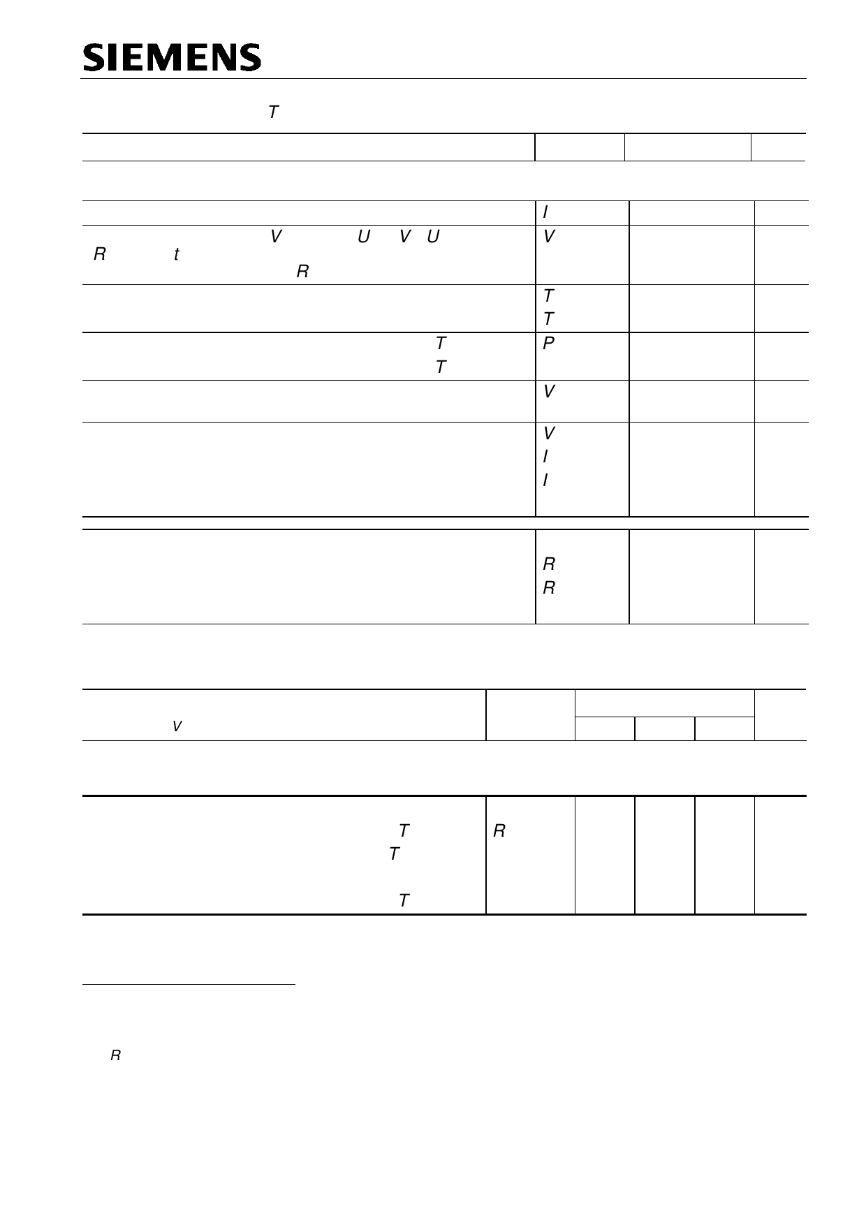
Maximum Ratings at Tj = 25°C unless otherwise specified
Parameter
Symbol
Values Unit
Load current (Short-circuit current, see page 5)
Load dump protection2) VLoadDump = UA + Vs, UA = 13.5 V
RI3) = 2 Ω, td = 200 ms; IN = low or high,
each channel loaded with RL = 3.4 Ω,
Operating temperature range
Storage temperature range
Power dissipation (DC)5
(all channels active)
Electrostatic discharge capability (ESD)
(Human Body Model)
Ta = 25°C:
Ta = 85°C:
Input voltage (DC)
Current through input pin (DC)
Current through status pin (DC)
see internal circuit diagram page 8
IL
VLoad dump4)
Tj
Tstg
Ptot
VESD
VIN
IIN
IST
Thermal resistance
junction - soldering point5),6)
junction - ambient5)
each channel: Rthjs
one channel active: Rthja
all channels active:
self-limited A
60 V
-40 ...+150 °C
-55 ...+150
3.7 W
1.9
1.0 kV
-10 ... +16 V
±2.0 mA
±5.0
12 K/W
41
34
Electrical Characteristics
Parameter and Conditions, each of the two channels
at Tj = 25 °C, Vbb = 12 V unless otherwise specified
Symbol
Values
Unit
min typ max
Load Switching Capabilities and Characteristics
On-state resistance (Vbb to OUT)
IL = 2 A
each channel, Tj = 25°C: RON
Tj = 150°C:
two parallel channels, Tj = 25°C:
-- 50 60 mΩ
100 120
25 30
2) Supply voltages higher than Vbb(AZ) require an external current limit for the GND and status pins, e.g. with a
150 Ω resistor in the GND connection and a 15 kΩ resistor in series with the status pin. A resistor for input
protection is integrated.
3) RI = internal resistance of the load dump test pulse generator
4) VLoad dump is setup without the DUT connected to the generator per ISO 7637-1 and DIN 40839
5) Device on 50mm*50mm*1.5mm epoxy PCB FR4 with 6cm2 (one layer, 70µm thick) copper area for Vbb
connection. PCB is vertical without blown air. See page 14
6) Soldering point: upper side of solder edge of device pin 15. See page 14
Semiconductor Group
3
Share Link: 