BUV48 View Datasheet(PDF) - Bourns, Inc
Part Name
Description
Manufacturer
BUV48 Datasheet PDF : 6 Pages
| |||
BUV48, BUV48A
NPN SILICON POWER TRANSISTORS
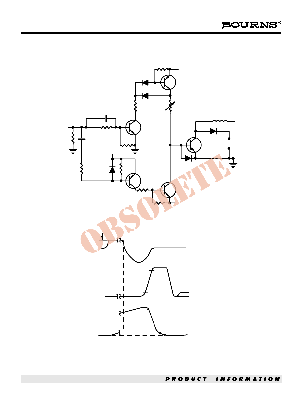
PARAMETER MEASUREMENT INFORMATION
33 Ω
+5V
BY205-400
D45H11
V Gen
68 Ω
BY205-400
33 Ω
1 pF
1 kΩ
0.02 µF
+5V
1 kΩ
2N2222
RB (on)
180 µH
vcc
TUT
BY205-400
Vclamp = 400 V
OBSOLETE 270 Ω BY205-400
1 kΩ
5X BY205-400
Adjust pw to obtain IC
For IC < 6 A VCC = 50 V
For IC ≥ 6 A VCC = 100 V
2N2904
47 Ω
100 Ω
D44H11
VBE(off)
Figure 3. Inductive-Load Switching Test Circuit
A - B = tsv
B - C = trv
IB(on)
IB
A (90%)
Base Current
D - E = tfi
E - F = tti
B - E = txo
C 90%
B 10%
VCE
Collector Voltage
D (90%)
E (10%)
I C(on)
F (2%)
Collector Current
NOTES: A. Waveforms are monitored on an oscilloscope with the following characteristics: tr < 15 ns, Rin > 10 Ω, Cin < 11.5 pF.
B. Resistors must be noninductive types.
Figure 4. Inductive-Load Switching Waveforms
PRODUCT INFORMATION
4
AUGUST 1978 - REVISED SEPTEMBER 2002
Specifications are subject to change without notice.
Share Link: 