HGLM-1063 View Datasheet(PDF) - HP => Agilent Technologies
Part Name
Description
Manufacturer
HGLM-1063 Datasheet PDF : 10 Pages
| |||
HPFC-5000
TACHYON
HGLM-1063
GIGABAUD OPTICAL
LINK MODULE
Tx
FIBER
Rx
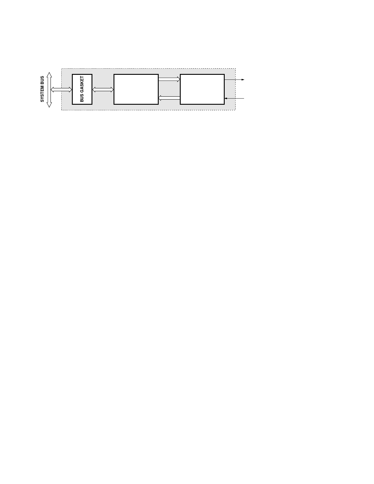
Figure 1. Example System Adapter Card, Block Diagram (Simplified).
Functional Description
A simplified block diagram of the
HGLM-1063 module is shown in
Figure 2. This block diagram
shows the 5 key elements of the
module. These are the Transmit-
ter I.C., the Laser Diode Assembly,
the Receiver I.C., the photodiode
assembly, and the Open Fiber
Control circuit. The high level of
integration on the HGLM-1063 is
apparent from this block
diagram. Pin assignments and
signal definitions are given on
pages 6 and 7.
In general, the HGLM-1063
utilizes a user provided Transmit
Byte Clock (TBC) of 53.125 MHz
to transmit two 8b/10b encoded
data bytes, simultaneously, by
creating a serial data stream of
1062.5 MBd and modulating a
780 nm laser diode with it. The
20 bit wide (two encoded bytes)
data input is provided to the
module through the 80 pin con-
nector in standard TTL format.
Similarly, the HGLM-1063
receives 780 nm optical signals at
a data rate of 1062.5 MBd,
deserializes this data stream to
recover the two encoded data
bytes and provides this 20 bit
wide standard TTL data to the
receiving system via the 80 pin
connector. The receiver also
recovers the byte rate clock for
use in clocking the received 20
bit wide parallel data.
Link Acquisition and
Power Up
The following discussion assumes
the HGLM-1063 is connected in a
full duplex point to point link as
shown in Figure 3. When initially
applying power to the HGLM-
1063, the Transmit Byte Clock
must start no later than 5 msec
after the +5 volt supply reaches
the +4 volt level. If this require-
ment is not met, the Open Fiber
Control (OFC) circuit may stick
in a nonfunctional state. If this
should happen, the OFC can be
put into a functional state by
holding the Enable Wrap
(EWRAP) line high for 10.5
seconds. Once the TBC is
running, and the module is
properly powered up, the follow-
ing sequence should be followed
to bring the link into full
synchronization and ready to
transmit data:
1. Both Link Unusable lines will
be driven high, by the OFC,
indicating neither receiver is
detecting a signal from the link.
2. Drive the Transmit Data lines,
Tx[00:19] to a
01010101010101010101.
3. Drive the input control lines as
follows:
• Enable Wrap: low
• Tx_SI: low
• Enable Comma Detect: high
• -Lock to Reference: high
4. Assuming the link is properly
connected, and both link ends are
in the same state of readiness, the
lasers will turn on in 10.1
seconds. This will be indicated by
the Link Unusable lines going
low. This transition indicates the
OFC is operational and in
control.
5. Once the lasers have come on,
and Link Unusable is observed to
transition low, bring -Lock to
Reference low for at least
500 µsec. This forces the module
to frequency lock to the Transmit
Byte Clock.
727
Share Link: 