HMT112R7AFP8C View Datasheet(PDF) - Hynix Semiconductor
Part Name
Description
Manufacturer
HMT112R7AFP8C Datasheet PDF : 41 Pages
| |||
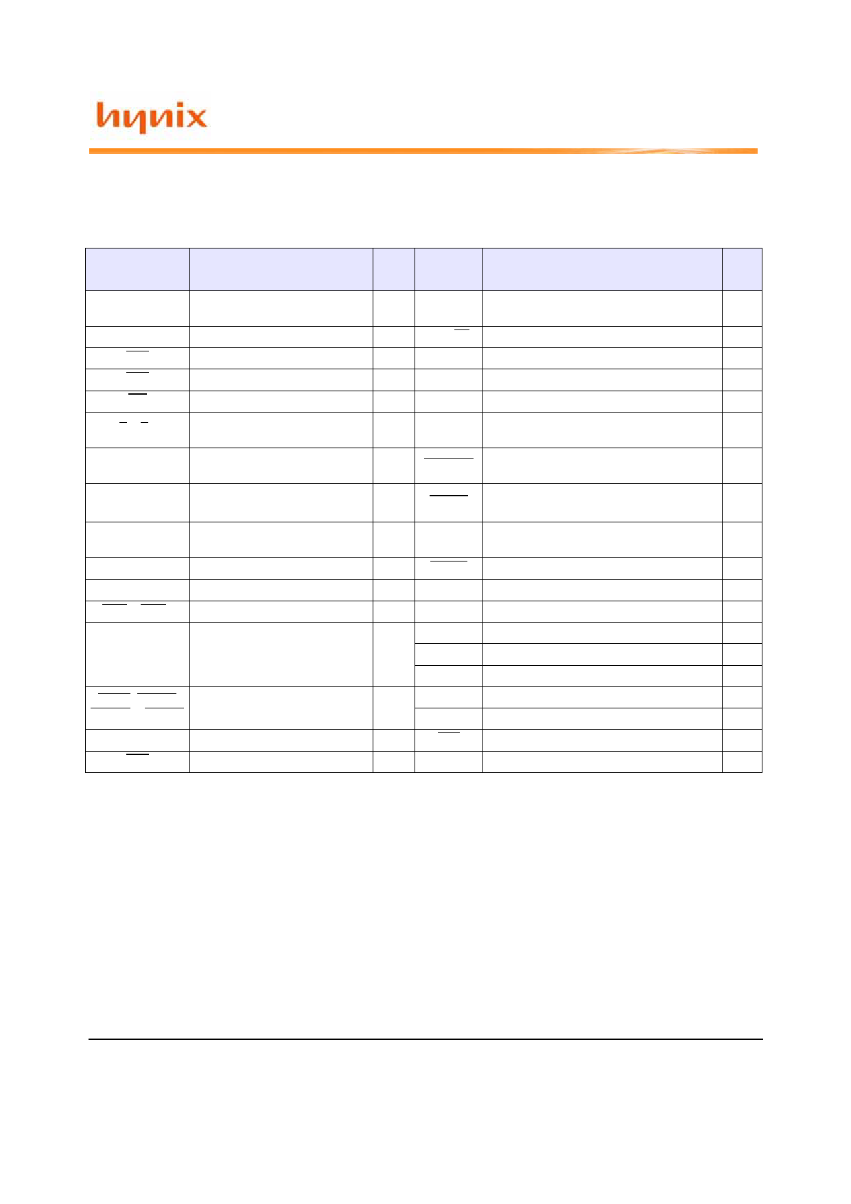
2. Pin Architecture
2.1 Pin Definition
Pin Name
A0–A9,A11
A13-A15
BA0–BA2
RAS
CAS
WE
S0–S3
Description
Address Inputs
SDRAM Bank Addresses
Row Address Strobe
Column Address Strobe
Write Enable
Chip Selects
CKE0–CKE1 Clock Enables
ODT0–ODT1 On-die termination Inputs
DQ0–DQ63 Data Input/Output
CB0–CB7
DQS0–DQS8
DQS0–DQS8
Data Check Bits Input/Output
Data Strobes
Data Strobes, Negative Line
DM0–DM8 Data Masks
DQS9-DQS17 Data Strobes
TDQS9-TDQS17 Termination Data Strobes
DQS9–DQS17 Data Strobes, Negative Line
TDQS9–TDQS17 Termination Data Strobes
CK0
Clock Input, positive line
CK0
Clock Input, positive Line
Num Pin
-ber Name
Description
Num
-ber
14 A10/AP Address Input/Autoprecharge
1
3 A12/BC Address Input/Autoprecharge
1
1
SCL Serial Presence Detect (SPD) Clock Input 1
1
SDA SPD Data Input/Output
1
1 SA0–SA2 SPD Address Inputs
3
4
Par_in
Parity Bit For The Address and Control
Bus
1
2
ERR_OUT
Parity Error Found on the Address and
Control Bus
1
2
EVENT
Reserved for Optional Hardware
temperature Sensing
1
64
TEST
Memory Bus Test Tool (Not Connected
and Not Usable on DIMMs)
1
8 RESET Register and SDRAM control pin
1
9
VDD Power Supply
22
9
VSS Ground
59
VREFDQ Reference Voltage for DQ
1
9 VREFCA Reference Voltage for CA
1
VTT Termination Voltage
4
VDDSPD SPD Power
1
9
CK1 Clock Input, positive line
1
1
CK1 Clock Input, negative line
1
1
Rev. 0.4 / Jul. 2009
6
Share Link: 