HY57V56820CLT View Datasheet(PDF) - Hynix Semiconductor
Part Name
Description
Manufacturer
HY57V56820CLT Datasheet PDF : 12 Pages
| |||
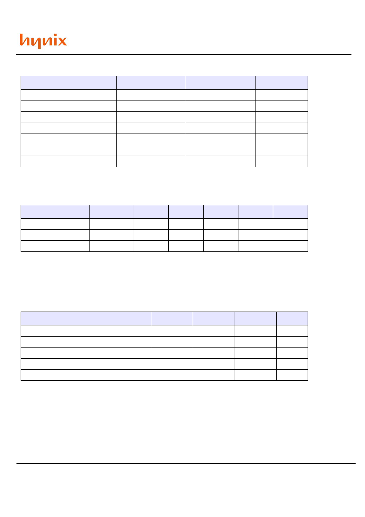
ABSOLUTE MAXIMUM RATINGS
Parameter
Ambient Temperature
Storage Temperature
Voltage on Any Pin relative to VSS
Voltage on VDD relative to VSS
Short Circuit Output Current
Power Dissipation
Soldering Temperature ⋅ Time
Symbol
TA
TSTG
VIN, VOUT
VDD, VDDQ
IOS
PD
TSOLDER
Rating
0 ~ 70
-55 ~ 125
-1.0 ~ 4.6
-1.0 ~ 4.6
50
1
260 ⋅ 10
Note : Operation at above absolute maximum rating can adversely affect device reliability
DC OPERATING CONDITION (TA=0 to 70°C)
Parameter
Power Supply Voltage
Input High Voltage
Input Low Voltage
Symbol
VDD, VDDQ
VIH
VIL
Min
3.0
2.0
- 0.3
Typ.
3.3
3.0
0
Note :
1.All voltages are referenced to VSS = 0V
2.VIH (max) is acceptable 5.6V AC pulse width with ≤3ns of duration
3.VIL (min) is acceptable -2.0V AC pulse width with ≤3ns of duration
Max
3.6
VDD + 0.3
0.8
AC OPERATING CONDITION (TA=0 to 70°C, VDD=3.3 ± 0.3V, VSS=0V)
Parameter
AC Input High / Low Level Voltage
Input Timing Measurement Reference Level Voltage
Input Rise / Fall Time
Output Timing Measurement Reference Level
Output Load Capacitance for Access Time Measurement
Symbol
VIH / VIL
Vtrip
tR / tF
Voutref
CL
Value
2.4/0.4
1.4
1
1.4
50
Note :
1. Output load to measure access time is equivalent to two TTL gates and one capacitor (50pF)
For details, refer to AC/DC output circuit
HY57V56820C(L)T
Unit
°C
°C
V
V
mA
W
°C ⋅ Sec
Unit
Note
V
1
V
1,2
V
1,3
Unit
Note
V
V
ns
V
pF
1
Rev. 0.4 / July 2003
4
Share Link: 