INT200TFI1 View Datasheet(PDF) - Power Integrations, Inc
Part Name
Description
Manufacturer
INT200TFI1
Power Integrations, Inc

INT200TFI1 Datasheet PDF : 12 Pages
| |||
INT200
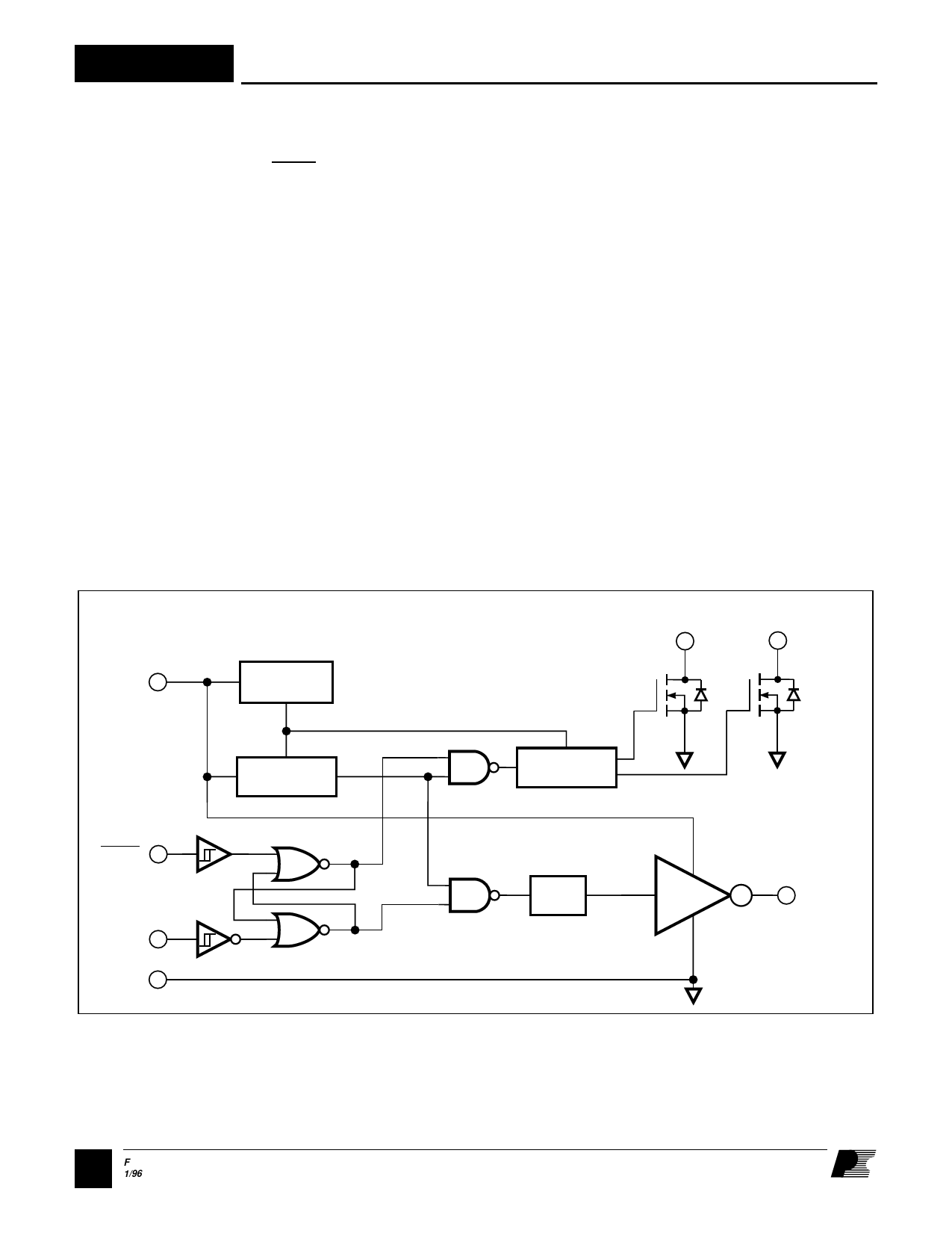
Pin Functional Description
Pin 1:
Active-low logic-level input HS IN
controls the pulse circuit which signals
the INT201 high-side driver.
Pin 2:
Active-high logic level input LS IN
controls the low side driver output.
Pin 3:
LS OUT is the driver output which
controls the low-side MOSFET.
Pin 4:
COM connection; analog reference point
for the circuit.
Pin 5:
Level shift output HSD 2 signals the
high-side driver to turn off. One short,
precise pulse is sent on each positive
transition of HS IN.
Pin 6:
Level shift output HSD 1 signals the
high-side driver to turn on. Two short,
precise pulses are sent on each negative
transition of HS IN.
Pin 7:
N/C for creepage distance.
Pin 8:
V supplies power to the logic, high-
DD
side interface, and low-side driver.
VDD
HS IN
LINEAR
REGULATOR
UV
LOCKOUT
LS IN
COM
Figure 3. Functional Block Diagram of the INT200
2F
1/96
HSD1
HSD2
PULSE
CIRCUIT
DELAY
LS OUT
PI-286F-043093
Share Link: