FP4229PBF View Datasheet(PDF) - International Rectifier
Part Name
Description
Manufacturer
FP4229PBF Datasheet PDF : 8 Pages
| |||
IRFP4229PbF
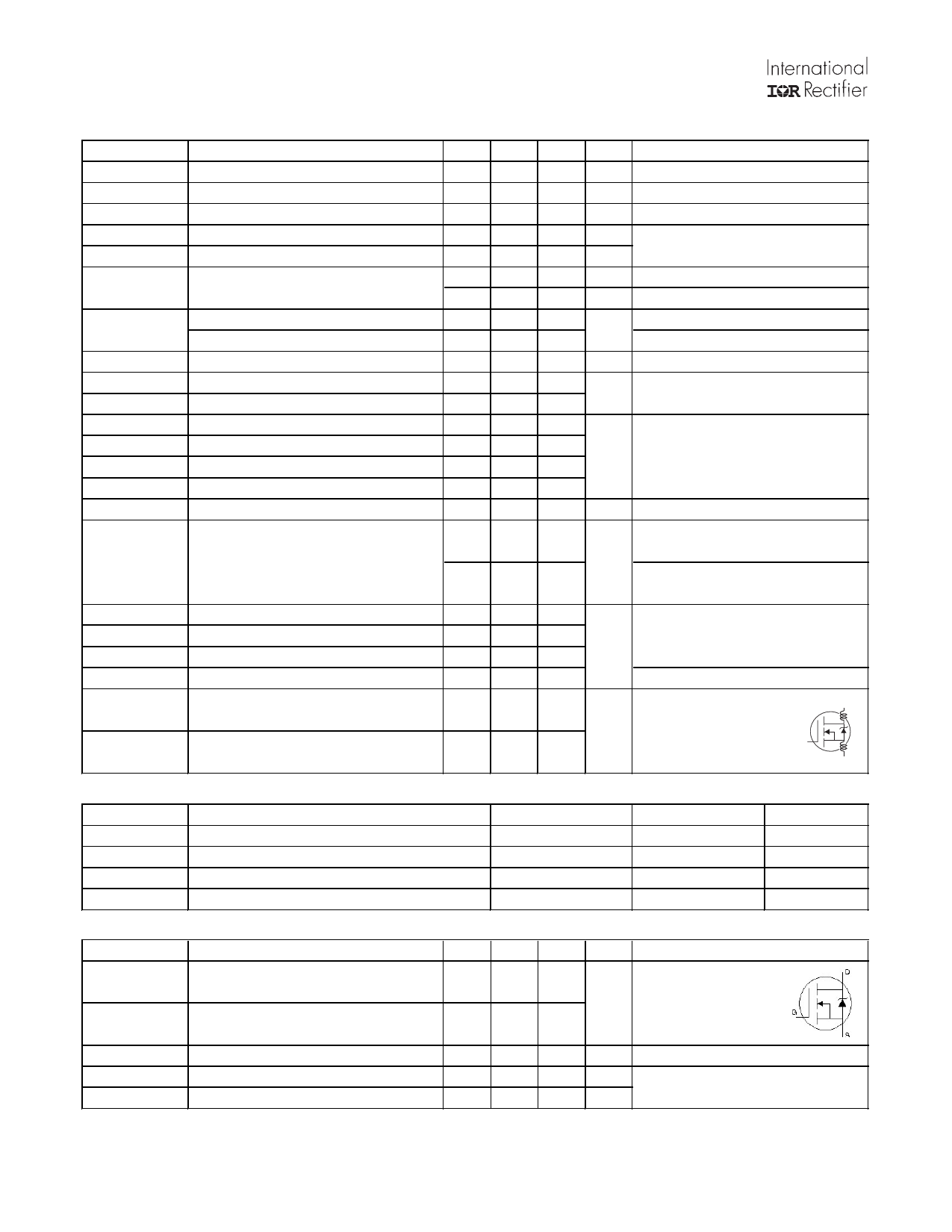
Electrical Characteristics @ TJ = 25°C (unless otherwise specified)
Parameter
Min. Typ. Max. Units
Conditions
BVDSS
Drain-to-Source Breakdown Voltage
250 ––– ––– V VGS = 0V, ID = 250µA
∆ΒVDSS/∆TJ
RDS(on)
Breakdown Voltage Temp. Coefficient
Static Drain-to-Source On-Resistance
–––
–––
210
38
e ––– mV/°C Reference to 25°C, ID = 1mA
46 mΩ VGS = 10V, ID = 26A
VGS(th)
Gate Threshold Voltage
3.0 ––– 5.0 V VDS = VGS, ID = 250µA
∆VGS(th)/∆TJ
IDSS
Gate Threshold Voltage Coefficient
Drain-to-Source Leakage Current
––– -14 ––– mV/°C
––– ––– 20 µA VDS = 250V, VGS = 0V
––– ––– 1.0 mA VDS = 250V, VGS = 0V, TJ = 125°C
IGSS
Gate-to-Source Forward Leakage
––– ––– 100 nA VGS = 20V
Gate-to-Source Reverse Leakage
––– ––– -100
VGS = -20V
gfs
Forward Transconductance
Qg
Total Gate Charge
83 ––– –––
––– 72 110
e S VDS = 25V, ID = 26A
nC VDD = 125V, ID = 26A, VGS = 10V
Qgd
Gate-to-Drain Charge
td(on)
Turn-On Delay Time
––– 26 –––
––– 25 –––
Ãe VDD = 125V, VGS = 10V
tr
Rise Time
––– 27 ––– ns ID = 26A
td(off)
Turn-Off Delay Time
––– 44 –––
RG = 5.0Ω
tf
Fall Time
––– 19 –––
See Fig. 22
tst
Shoot Through Blocking Time
100 ––– ––– ns VDD = 200V, VGS = 15V, RG= 4.7Ω
EPULSE
Energy per Pulse
––– 790 –––
L = 220nH, C= 0.3µF, VGS = 15V
µJ VDS = 200V, RG= 4.7Ω, TJ = 25°C
––– 1390 –––
L = 220nH, C= 0.3µF, VGS = 15V
VDS = 200V, RG= 4.7Ω, TJ = 100°C
Ciss
Input Capacitance
––– 4560 –––
VGS = 0V
Coss
Output Capacitance
––– 390 ––– pF VDS = 25V
Crss
Reverse Transfer Capacitance
––– 100 –––
ƒ = 1.0MHz,
Coss eff.
Effective Output Capacitance
––– 290 –––
VGS = 0V, VDS = 0V to 200V
LD
Internal Drain Inductance
––– 5.0 –––
Between lead,
D
nH 6mm (0.25in.)
LS
Internal Source Inductance
––– 13 –––
from package
G
and center of die contact
S
Avalanche Characteristics
EAS
EAR
VDS(Avalanche)
IAS
Parameter
d Single Pulse Avalanche Energy
Repetitive Avalanche Energy
à Repetitive Avalanche Voltage
Ãd Avalanche Current
Diode Characteristics
Parameter
IS @ TC = 25°C Continuous Source Current
(Body Diode)
ISM
Pulsed Source Current
à (Body Diode)
VSD
Diode Forward Voltage
trr
Reverse Recovery Time
Qrr
Reverse Recovery Charge
Typ.
Max.
Units
–––
300
mJ
–––
31
mJ
300
–––
V
–––
26
A
Min.
–––
–––
–––
–––
–––
Typ.
–––
–––
–––
190
840
Max. Units
Conditions
44
MOSFET symbol
A showing the
180
integral reverse
1.3
290
1260
p-n junction diode.
e V TJ = 25°C, IS = 26A, VGS = 0V
ns TJ = 25°C, IF = 26A, VDD = 50V
e nC di/dt = 100A/µs
2
www.irf.com
Share Link: 