LT1166 View Datasheet(PDF) - Linear Technology
Part Name
Description
Manufacturer
LT1166 Datasheet PDF : 16 Pages
| |||
LT1166
ABSOLUTE MAXIMUM RATINGS
Supply Current (Pin 1 or Pin 4) ............................ 75mA
Differential Voltage (Pin 2 to Pin 3) ......................... ±6V
Output Short-Circuit Duration (Note 1) ......... Continuous
Specified Temperature Range (Note 2) ........ 0°C to 70°C
Operating Temperature Range ................ – 40°C to 85°C
Storage Temperature Range ................. – 65°C to 150°C
Junction Temperature (Note 3) ............................ 150°C
Lead Temperature (Soldering, 10 sec).................. 300°C
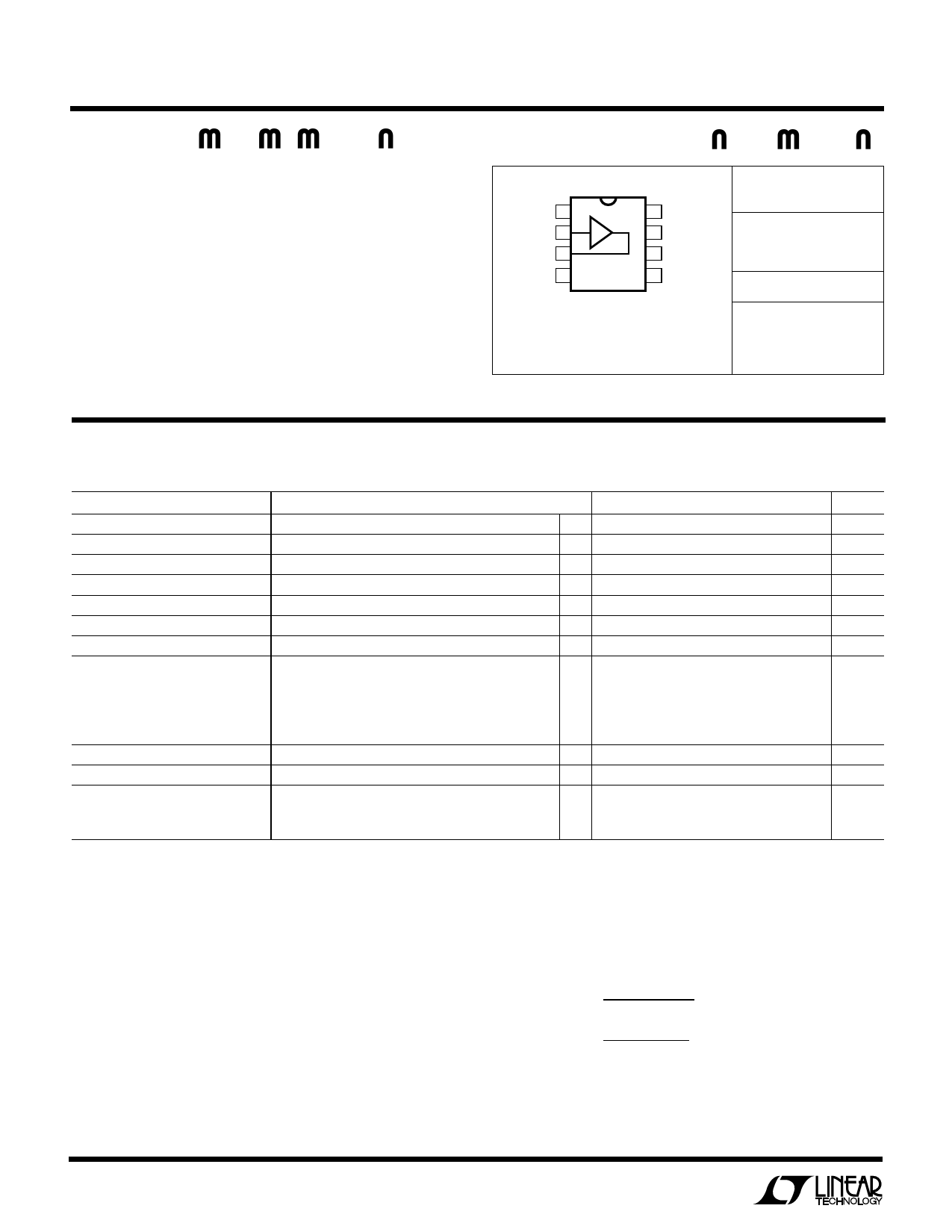
PACKAGE/ORDER INFORMATION
VTOP 1
VIN 2
VOUT 3
VBOTTOM 4
TOP VIEW
+1
8 SENSE+
7 ILIM+
6 ILIM–
5 SENSE–
N8 PACKAGE
8-LEAD PDIP
S8 PACKAGE
8-LEAD PLASTIC SO
TJMAX = 150°C, θJA = 100°C/ W (N8)
TJMAX = 150°C, θJA = 150°C/ W (S8)
ORDER PART
NUMBER
LT1166CN8
LT1166CS8
S8 PART MARKING
1166
Consult factory for Industrial and Military grade parts.
ELECTRICAL CHARACTERISTICS
Pin 1 = 2V, Pin 4 = – 2V, Operating current 15mA and RIN = 20k, unless otherwise specified.
PARAMETER
Output Offset Voltage
Input Bias Current
Input Resistance
VAB (Top)
VAB (Bottom)
Voltage Compliance
Current Compliance
Transconductance
gmCC2
gmEE2
gmCC10
gmEE10
PSRRCC
PSRREE
Current Limit Voltage
CONDITIONS
Operating Current 15mA to 50mA
Operating Current 15mA to 50mA (Note 4)
Operating Current 15mA to 50mA (Note 5)
Measure Pin 8 to Pin 3, No Load
Measure Pin 5 to Pin 3, No Load
Operating Current = 50mA (Notes 6, 9)
Operating Voltage = ±2V
(Note 7)
Pin 1 = 2V, Pin 4 = – 2V
Pin 1 = 2V, Pin 4 = – 2V
Pin 1 = 10V, Pin 4 = – 10V
Pin 1 = 10V, Pin 4 = – 10V
(Note 8)
(Note 8)
Operating Current 15mA to 50mA
Pin 7 Voltage to Pin 3
Pin 6 Voltage to Pin 3
MIN
q
q
q
2
14
– 14
q
±2
q
±4
q
0.08
q
0.08
q
0.09
q
0.09
q
1.0
q
– 1.0
TYP
50
2
15
20
– 20
0.100
0.100
0.125
0.125
19
19
1.3
– 1.3
MAX
UNITS
250
mV
10
µA
MΩ
26
mV
– 26
mV
± 10
V
± 50
mA
0.13
mho
0.13
mho
0.16
mho
0.16
mho
dB
dB
1.5
V
– 1.5
V
The q denotes specifications which apply over the full operating
temperature range.
Note 1: External power devices may require heat sinking.
Note 2: Commercial grade parts are designed to operate over the
temperature range of – 40°C to 85°C but are neither tested nor guaranteed
beyond 0°C to 70°C. Industrial grade parts specified and tested over
– 40°C and 85°C are available on special request, consult factory.
Note 3: TJ calculated from the ambient temperature TA and the power
dissipation PD according to the following formulas:
LT1166CN8: TJ = TA + (PD • 100°C/W)
LT1166CS8: TJ = TA + (PD • 150°C/W)
Note 4: ITOP = IBOTTOM
Note 5: The input resistance is typically 15MΩ when the loop is closed.
When the loop is open (current limit) the input resistance drops to 200Ω
referred to Pin 3.
Note 6: Maximum TJ can be exceeded with 50mA operating current and
simultaneous 10V and – 10V (20V total).
Note 7: Apply ±200mV to Pin 2 and measure current change in Pin 1
and 4. Pin 3 is grounded.
Note 8: PSRRCC = gmCC2 – gmCC10
gm CC2
PSRREE = gmEE2 – gmEE10
gm EE2
Note 9: For Linear Operation, Pin 1 must not be less than 2V or more than
10V from Pin 3. Similarly, Pin 4 must not be less than 2V or more than
10V from Pin 3.
2
Share Link: 