LTC4263CDE View Datasheet(PDF) - Linear Technology
Part Name
Description
Manufacturer
LTC4263CDE Datasheet PDF : 28 Pages
| |||

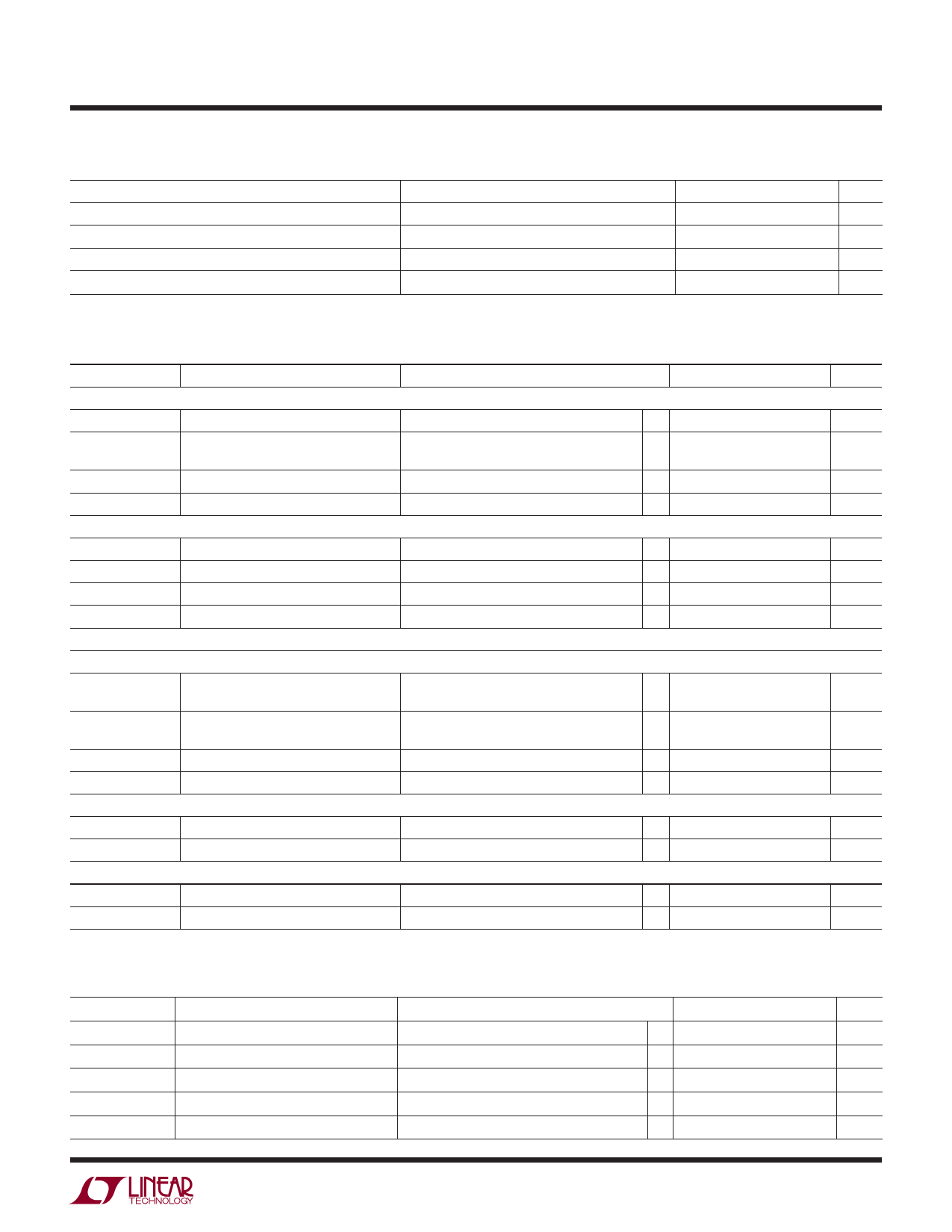
LTC2205-14
COMMON MODE BIAS CHARACTERISTICS The ● denotes the specifications which apply over
the full operating temperature range, otherwise specifications are at TA = 25°C. (Note 4)
PARAMETER
CONDITIONS
MIN
TYP
MAX UNITS
VCM Output Voltage
VCM Output Tempco
VCM Line Regulation
VCM Output Resistance
IOUT = 0
IOUT = 0
3.135V ≤ VDD ≤ 3.465V
1mA ≤ | IOUT | ≤ 1mA
1.15 1.25 1.35
V
±40
ppm/°C
1
mV/ V
1
Ω
DIGITAL INPUTS AND DIGITAL OUTPUTS The ● denotes the specifications which apply over the
full operating temperature range, otherwise specifications are at TA = 25°C. (Note 4)
SYMBOL
PARAMETER
ENCODE INPUTS (ENC+, ENC–)
CONDITIONS
MIN
TYP
MAX UNITS
VID
Differential Input Voltage (Note 7)
VICM
Common Mode Input Voltage
Internally Set
Externally Set (Note 7)
l 0.2
V
1.6
V
1.2
3.0
V
RIN
Input Resistance
(See Figure 2)
6
kΩ
CIN
Input Capacitance
LOGIC INPUTS (DITH, PGA, SHDN, RAND)
(Note 7)
3
pF
VIH
VIL
IIN
CIN
LOGIC OUTPUTS
High Level Input Voltage
Low Level Input Voltage
Digital Input Current
Digital Input Capacitance
VDD = 3.3V
VDD = 3.3V
VIN = 0V to VDD
(Note 7)
l2
V
l
0.8
V
l
±10
μA
1.5
pF
OVDD = 3.3V
VOH
VOL
ISOURCE
High Level Output Voltage
Low Level Output Voltage
Output Source Current
VDD = 3.3V
VDD = 3.3V
VOUT = 0V
IO = –10μA
3.299
V
IO = –200μA l 3.1
3.29
V
IO = –160μA
IO = –1.6μA l
0.01
V
0.10
0.4
V
–50
mA
ISINK
OVDD = 2.5V
VOH
VOL
OVDD = 1.8V
VOH
Output Sink Current
High Level Output Voltage
Low Level Output Voltage
High Level Output Voltage
VOUT = 3.3V
VDD = 3.3V
VDD = 3.3V
VDD = 3.3V
IO = –200μA
IO = 1.60mA
IO = –200μA
50
mA
2.49
V
0.1
V
1.79
V
VOL
Low Level Output Voltage
VDD = 3.3V
IO = 1.60mA
0.1
V
POWER REQUIREMENTS The ● denotes the specifications which apply over the full operating temperature
range, otherwise specifications are at TA = 25°C. (Note 4)
SYMBOL
PARAMETER
CONDITIONS
MIN TYP MAX UNITS
VDD
Analog Supply Voltage
3.315 3.3 3.465
V
PSHDN
Shutdown Power
SHDN = VDD
0.2
mW
OVDD
Output Supply Voltage
l 0.5
3.3
3.6
V
IVDD
Analog Supply Current
l
181
212
mA
PDIS
Power Dissipation
l
597
700
mW
220514fb
5