LTC4263IDE View Datasheet(PDF) - Linear Technology
Part Name
Description
Manufacturer
LTC4263IDE Datasheet PDF : 28 Pages
| |||
LTC2205-14
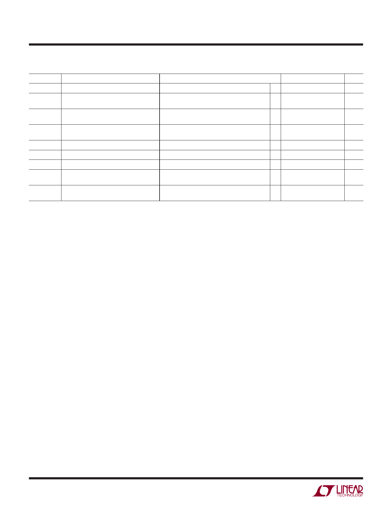
TIMING CHARACTERISTICS The ● denotes the specifications which apply over the full operating temperature
range, otherwise specifications are at TA = 25°C. (Note 4)
SYMBOL
fS
tL
tH
tAP
tD
tC
tSKEW
tOE
Pipeline
Latency
PARAMETER
Sampling Frequency
ENC Low Time
ENC High Time
Sample-and-Hold
Aperture Delay
ENC to DATA Delay
ENC to CLKOUT Delay
DATA to CLKOUT Skew
DATA Access Time
Bus Relinquish Time
CONDITIONS
Duty Cycle Stabilizer Off (Note 7)
Duty Cycle Stabilizer On (Note 7)
Duty Cycle Stabilizer Off (Note 7)
Duty Cycle Stabilizer On (Note 7)
(Note 7)
(Note 7)
(tD – tC) (Note 7)
CL = 5pf (Note 7)
(Note 7)
MIN
l1
l 6.40
l 4.60
l 6.40
l 4.60
l 1.3
l 1.3
l –0.6
l
l
TYP MAX UNITS
65
MHz
7.69 500
ns
7.69 500
ns
7.69 500
ns
7.69 500
ns
0.7
ns
2.7 4.0
ns
2.7 4.0
ns
0
0.6
ns
5
15
ns
5
15
ns
7
Cycles
Note 1: Stresses beyond those listed under Absolute Maximum Ratings
may cause permanent damage to the device. Exposure to any Absolute
Maximum Rating condition for extended periods may affect device
reliability and lifetime.
Note 2: All voltage values are with respect to GND, with GND and OGND
shorted (unless otherwise noted).
Note 3: When these pin voltages are taken below GND or above VDD, they
will be clamped by internal diodes. This product can handle input currents
of greater than 100mA below GND or above VDD without latchup.
Note 4: VDD = 3.3V, fSAMPLE = 65MHz differential ENC+/ENC– = 2VP-P sine
wave with 1.6V common mode, input range = 2.25VP-P with differential
drive (PGA = 0), unless otherwise specified.
Note 5: Integral nonlinearity is defined as the deviation of a code from
a “best fit straight line” to the transfer curve. The deviation is measured
from the center of the quantization band.
Note 6: Offset error is the offset voltage measured from –1/2LSB when the
output code flickers between 00 0000 0000 0000 and 11 1111 1111 1111
in 2’s complement output mode.
Note 7: Guaranteed by design, not subject to test.
220514fb
6
Share Link: 