LTC2900 View Datasheet(PDF) - Linear Technology
Part Name
Description
Manufacturer
LTC2900 Datasheet PDF : 16 Pages
| |||
LTC2900
ELECTRICAL CHARACTERISTICS The q denotes the specifications which apply over the full operating
temperature range, otherwise specifications are at TA = 25°C. VCC = 5V, unless otherwise noted. (Note 3)
SYMBOL PARAMETER
CONDITIONS
MIN TYP MAX UNITS
IV2
V2 Input Current
IV3
V3 Input Current
V2 = 3.3V
V3 = 2.5V
V3 = 0.55V (ADJ Mode)
q
0.8
2
µA
q
0.52
1.2
µA
q
–15
15
nA
IV4
V4 Input Current
V4 = 1.8V
V4 = 0.55V (ADJ Mode)
V4 = –0.05V (–ADJ Mode)
q
0.34
0.8
µA
q
–15
15
nA
q
– 15
15
nA
ICRT(UP)
ICRT(DN)
CRT Pull-Up Current
CRT Pull-Down Current
VCRT = 0V
VCRT = 1.3V
q
– 1.4
–2
– 2.6
µA
q
10
20
30
µA
tRST
Reset Time-Out Period
tUV
VX Undervoltage Detect to RST
CRT = 1500pF
q
5
7
9
ms
VX Less Than Reset Threshold VRTX
by More Than 1%
150
µs
VOL
Output Voltage Low RST
ISINK = 2.5mA; V1 = 3V, V2 = 3V;
q
V3, V4 = 0V; VPG = 0V
0.15
0.4
V
ISINK = 100µA; V2 = 1V; V1, V3, V4 = 0V q
ISINK = 100µA; V1 = 1V; V2, V3, V4 = 0V q
0.05
0.3
V
0.05
0.3
V
VOH
Output Voltage High RST (LTC2900-1)
ISOURCE = 1µA
q V2 – 1
V
(Note 5)
Output Voltage High RST (LTC2900-2)
ISOURCE = 200µA
q 0.8 • V2
V
(Note 6)
Manual Reset Pin
VIH
PBR Input Threshold High
VIL
PBR Input Threshold Low
tPBW
PBR Input Pulse Width
tPBD
Manual Reset Propagation Delay
IPBR
PBR Pull-Up Current
VCC = 3.3V to 5.5V
VCC = 3.3V to 5.5V
VCC = 3.3V
VCC = 3.3V, VPBR Falling
VPBR = 0V
q
1.6
V
q
0.4
V
q
150
ns
q
0.1
1
µs
– 10
µA
Note 1: Absolute Maximum Ratings are those values beyond which the life of
a device may be impaired.
Note 2: All currents into pins are positive, all voltages are referenced to GND
unless otherwise noted.
Note 3: The greater of V1, V2 is the internal supply voltage (VCC).
Note 4: Under static no-fault conditions, V1 will necessarily supply quiescent
current. If at any time V2 is larger than V1, V2 must be capable of supplying
the quiescent current, programming (transient) current and reference load
current.
Note 5: The RST output pin on the LTC2900-1 has an internal pull-up to V2
of typically 6µA. However, an external pull-up resistor may be used when
faster rise times are required or for VOH voltages greater than V2.
Note 6: The push-pull RST output pin on the LTC2900-2 is actively pulled up
to V2.
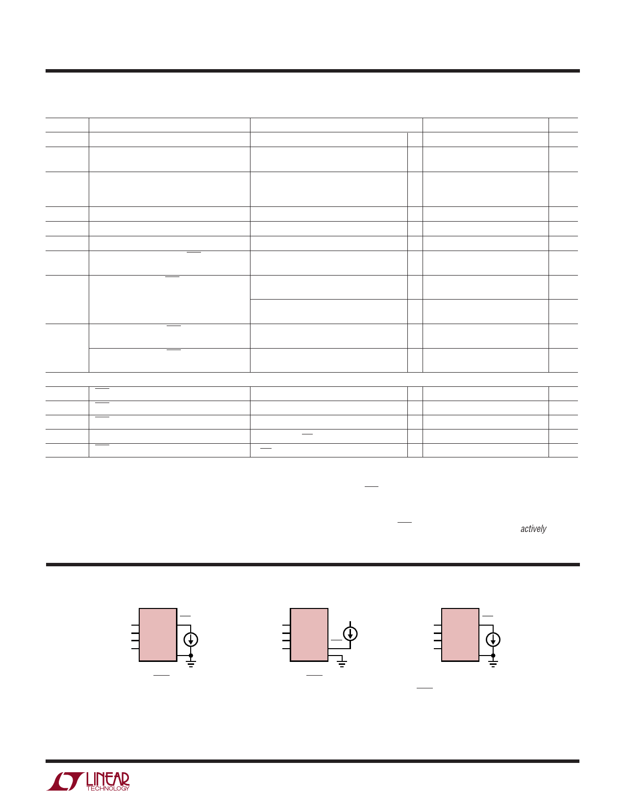
TEST CIRCUITS
LTC2900-1 RST
V1
V2
V3
ISOURCE
1µA
V4
2900 F01
Figure 1. RST VOH Test
LTC2900-1
V1
V2
V3
V4
RST
ISINK
2.5mA,
100µA
2900 F02
Figure 2. RST VOL Test
LTC2900-2 RST
V1
V2
V3
ISOURCE
200µA
V4
2900 F03
Figure 3. Active Pull-Up
RST VOH Test
2900f
3
Share Link: 