M1025-1026 View Datasheet(PDF) - Analog Devices
Part Name
Description
Manufacturer
M1025-1026 Datasheet PDF : 16 Pages
| |||
ADM1025/ADM1025A
Table IV. Controlling the Operation of INT
Test Register
Bit 1
Bit 0
Function
0
0
Interrupts Disabled
0
1
Thermal Interrupt Only
1
0
Voltage Interrupt Only
1
1
Voltage and Thermal Interrupts
Note that Bit 7 of VID register should be zero, and that Bits 2 to 7 of Test
Register must be zeros.
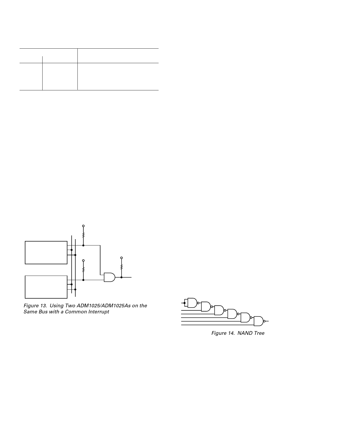
When Pin 16 is used as a RST or INT output, it is open-drain and
requires an external pull-up resistor. This will restrict the address
function on Pin 16 to being high at power-up. If the RST or INT
function is required and two ADM1025/ADM1025As are to be
used on the same serial bus, A1/A0 can be set to 10 by using a
high value pull-up on Pin 16 (100 kΩ or greater). This will not
override the “floating” condition of ADD during power-up.
Note, however, that the RST/INT outputs of two or more
devices cannot be wire-OR’d, as the devices would then have
the same address. If the RST/INT outputs need to be connected
to a common interrupt line, they can be OR’d together using the
circuit of Figure 13.
If the RST or INT functionality is not required, a third address
may be used by setting A1/A0 to 00 by using a 1 kΩ pull-down
resistor on Pin 16. Note that this address should not be used if
RST or INT is required, since using this address will cause the
device to appear to be generating resets or interrupts, since Pin
16 will be permanently tied low.
VCC
A1/A0 = 01
ADD/RST/INT/NTO
ADM1025/ SDA
ADM1025A SCL
#1
A1/A0 = 10
ADD/RST/INT/NTO
ADM1025/ SDA
ADM1025A SCL
#2
R1
1k⍀
VCC
R2
470k⍀
VCC
R5
4.7k⍀
RST OR INT
OPEN-COLLECTOR
AND GATE
Figure 13. Using Two ADM1025/ADM1025As on the
Same Bus with a Common Interrupt
GENERATING AN SMBALERT
The INT output can be used as an interrupt output or can be
used as an SMBALERT. One or more INT outputs can be con-
nected to a common SMBALERT line connected to the master.
If a device’s INT line goes low, the following procedure occurs:
1. SMBALERT pulled low.
2. Master initiates a read operation and sends the Alert
Response Address (ARA = 0001 100). This is a general call
address that must not be used as a specific device address.
3. The device whose INT output is low responds to the Alert
Response Address, and the master reads its device address.
The address of the device is now known and it can be inter-
rogated in the usual way.
4. If more than one device’s INT output is low, the one with
the lowest device address will have priority, in accordance
with normal SMBus arbitration.
5. Once the ADM1025/ADM1025A has responded to the Alert
Response Address, it will reset its INT output; however, if
the error condition that caused the interrupt persists, INT
will be reasserted on the next monitoring cycle.
NAND TREE TESTS
A NAND tree is provided in the ADM1025/ADM1025A for
Automated Test Equipment (ATE) board level connectivity
testing. The device is placed into NAND Test Mode by power-
ing up with Pin 9 (D-/NTI) held high. This pin is automatically
sampled after power-up and if it is connected high, the NAND
test mode is invoked.
In NAND test mode, all digital inputs may be tested as illus-
trated below. ADD/RST/INT/NTO will become the NAND test
output pin.
To perform a NAND tree test, all pins are initially driven low.
The test vectors set all inputs low, then one-by-one toggle them
high (keeping them high). Exercising the test circuit with this
“walking one” pattern, starting with the input closest to the out-
put of the tree, cycling toward the farthest, causes the output of
the tree to toggle with each input change. Allow for a typical
propagation delay of 500 ns. The structure of the NAND tree is
shown in Figure 14.
SDA
SCL
VID0
VID1
VID2
VID3
ADD/RST/INT/NTO
Figure 14. NAND Tree
Note: If any of the inputs shown in Figure 14 are unused, they
should not be connected directly to ground, but via a resistor
such as 10 kΩ. This will allow the ATE (Automatic Test Equip-
ment) to drive every input high so that the NAND tree test can
be properly carried out. Refer to Table XVI for Test Vectors.
–12–
REV. A
Share Link: 