M1025-1026 View Datasheet(PDF) - Analog Devices
Part Name
Description
Manufacturer
M1025-1026 Datasheet PDF : 16 Pages
| |||
ADM1025/ADM1025A
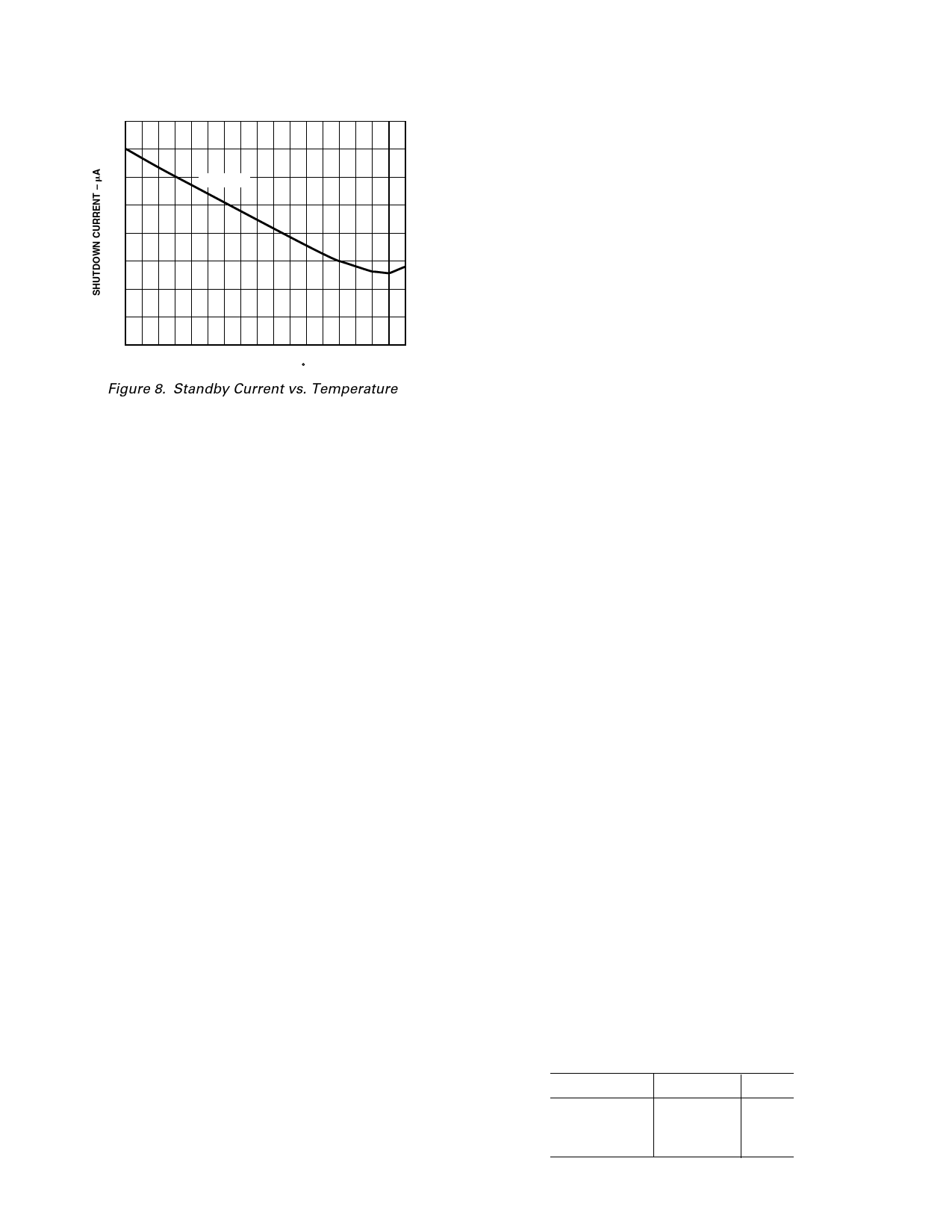
26.5
26.0
25.5
25.0
VDD = 3.3V
24.5
24.0
23.5
23.0
22.5
–40 –20 0
20 40 60 80 100 120
TEMPERATURE – C
Figure 8. Standby Current vs. Temperature
GENERAL DESCRIPTION
The ADM1025/ADM1025A is a complete system hardware
monitor for microprocessor-based systems. The device commu-
nicates with the system via a serial System Management Bus.
The serial bus controller has a hardwired address line for device
selection (Pin 16), a serial data line for reading and writing
addresses and data (Pin 1), and an input line for the serial clock
(Pin 2). All control and programming functions of the ADM1025/
ADM1025A are performed over the serial bus.
MEASUREMENT INPUTS
The device has six measurement inputs, five for voltage and one
for temperature. It can also measure its own supply voltage and
can measure ambient temperature with its on-chip temperature
sensor.
Pins 11 through 15 are analog inputs with on-chip attenuators,
configured to monitor 12 V, 5 V, 3.3 V, 2.5 V and the processor
core voltage, respectively. Pin 11 may alternatively be programmed
as a digital input for Bit 4 of the processor voltage ID code.
Power is supplied to the chip via Pin 4 and the system also
monitors the voltage on this pin.
Remote temperature sensing is provided by the D+ and D–
inputs, to which a diode-connected, external temperature-
sensing transistor may be connected.
An on-chip bandgap temperature sensor monitors system ambi-
ent temperature.
SEQUENTIAL MEASUREMENT
When the ADM1025/ADM1025A monitoring sequence is started,
it cycles sequentially through the measurement of analog inputs
and the temperature sensors. Measured values from these inputs
are stored in Value Registers. These can be read out over the
serial bus, or can be compared with programmed limits stored
in the Limit Registers. The results of out-of-limit comparisons
are stored in the Status Registers, which can be read over the
serial bus to flag out of limit conditions.
PROCESSOR VOLTAGE ID
Five digital inputs (VID4 to VID0—Pins 5 to 8 and 11) read the
processor voltage ID code and store it in the VID registers, from
which it can be read out by the management system over the
serial bus. If Pin 11 is configured as a 12 V analog input (power-
up default), the VID4 bit in the VID4 register will default to 0.
The VID pins have internal 100 kΩ pull-up resistors (ADM1025
only).
ADD/RST/INT/NTO
Pin 16 is a programmable digital I/O pin. After power-up, at the
first sign of SMBus activity, it is sampled to set the lowest two
bits of the serial bus address. During board-level, NAND tree
connectivity testing, this pin functions as the output of the NAND
tree. During normal operation Pin 16 may be programmed as a
reset output to provide a low going 20 ms reset pulse when
enabled, or it may be programmed as an interrupt output for
out-of-limit temperature and/or voltage events. These functions
are described in more detail later.
INTERNAL REGISTERS OF THE ADM1025/ADM1025A
A brief description of the ADM1025/ADM1025A’s principal
internal registers is given below. More detailed information on
the function of each register is given in Tables V to XV.
Configuration Register: Provides control and configuration.
Address Pointer Register: This register contains the address that
selects one of the other internal registers. When writing to the
ADM1025/ADM1025A, the first byte of data is always a register
address, which is written to the Address Pointer Register.
Status Registers: Two registers to provide status of each limit
comparison.
VID Registers: The status of the VID0 to VID4 pins of the
processor can read from these registers.
Value and Limit Registers: The results of analog voltage
inputs and temperature measurements are stored in these regis-
ters, along with their limit values.
Offset Register: Allows either an internal or external tempera-
ture channel reading to be offset by a two’s complement value
written to this register.
SERIAL BUS INTERFACE
Control of the ADM1025/ADM1025A is carried out via the
serial bus. The ADM1025/ADM1025A is connected to this
bus as a slave device, under the control of a master device or
master controller.
The ADM1025/ADM1025A has a 7-bit serial bus address. When
the device is powered up, it will do so with a default serial bus
address. The five MSBs of the address are set to 01011, the two
LSBs are determined by the logical states of Pin 16 at power-up.
This is a three-state input that can be grounded, connected to
VCC or left open-circuit to give three different addresses:
Table I. Address Selection
ADD Pin
A1
A0
GND
0
0
No Connect
1
0
VCC
0
1
–6–
REV. A
Share Link: 