M34280M1-XXXFP View Datasheet(PDF) - Renesas Electronics
Part Name
Description
Manufacturer
M34280M1-XXXFP
Renesas Electronics

M34280M1-XXXFP Datasheet PDF : 48 Pages
| |||
MITSUBISHI MICROCOMPUTERS
4280 Group
SINGLE-CHIP 4-BIT CMOS MICROCOMPUTER for INFRARED REMOTE CONTROL TRANSMITTERS
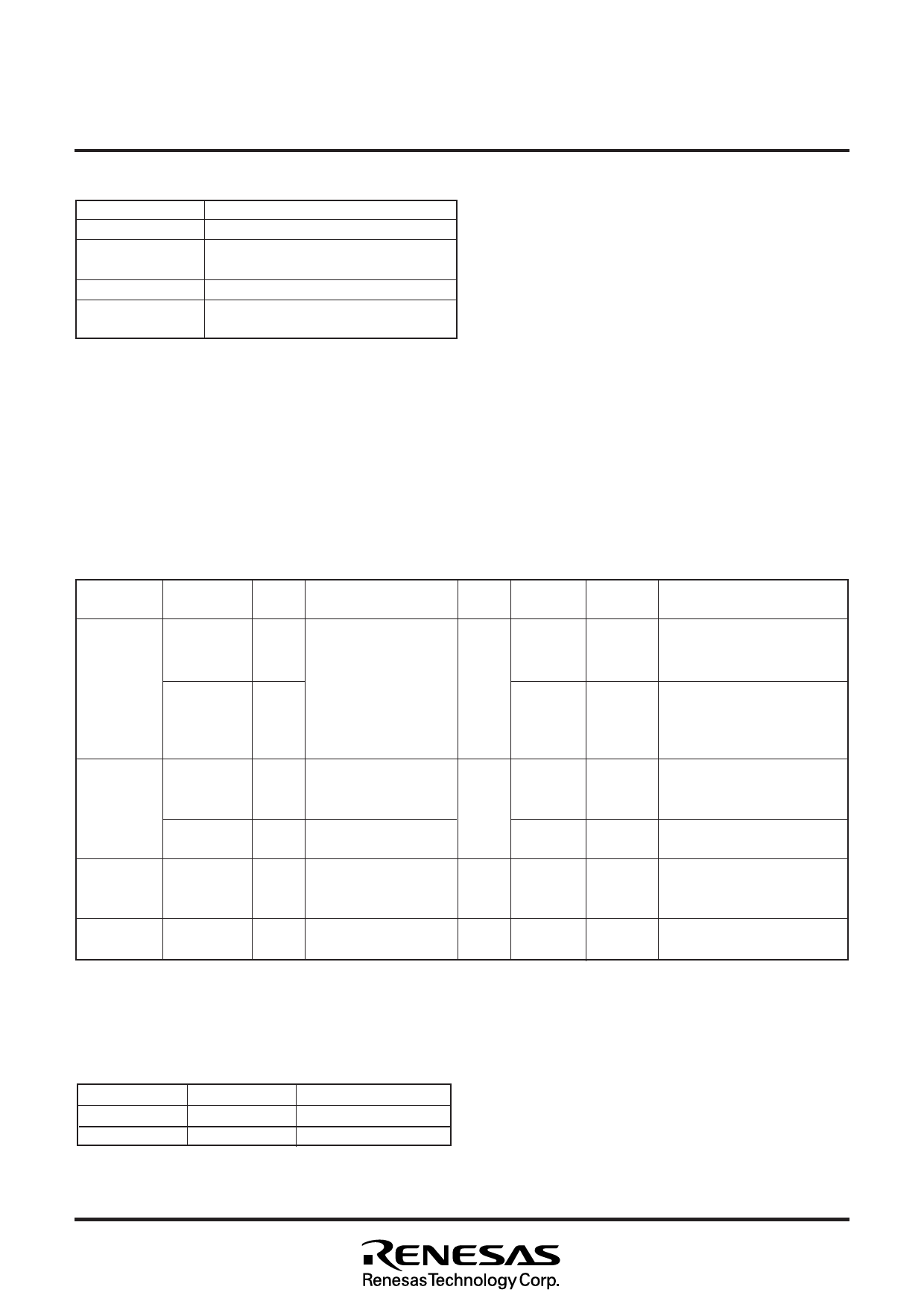
CONNECTIONS OF UNUSED PINS
Pin
Connection
D0–D7
Open or connect to VDD pin (Note 1).
E0, E1
Set the output latch to “1” and open, or
connect to VDD pin (Note 2).
E2
Open or connect to VSS pin.
G0–G3
Set the output latch to “0” and open, or
connect to VSS pin.
Notes 1: Port D7: Set the bit 2 (PU02) of the pull-down control register PU0 to “0” by software and turn the pull-down transistor OFF.
2: Set the corresponding bits (PU00, PU01) of the pull-down control register PU0 to “0” by software and turn the pull-down
transistor OFF.
(Note in order to set the output latch to “0” to make pins open)
• After system is released from reset, a port is in a high-impedance state until the output latch of the port is set to “0” by software.
Accordingly, the voltage level of pins is undefined and the excess of the supply current may occur.
• To set the output latch periodically is recommended because the value of output latch may change by noise or a program run away
(caused by noise).
(Note when connecting to VSS and VDD)
• Connect the unused pins to VSS or VDD at the shortest distance and use the thick wire against noise.
PORT FUNCTION
Port
Pin
Port D
D0–D6
D7
Port E
Port G
E0
E1
E2
G0–G3
Input/
Output
Output structure
Output P-channel open-drain
(7)
I/O
(1)
I/O P-channel open-drain
(2)
Input
(1)
I/O
(4)
P-channel open-drain
Control Control Control
bits instructions registers
1 bit SD
RD
CLD
SD
PU0
RD
CLD
SZD
Output: OEA
PU0
2 bits IAE
Input:
3 bits IAE
Remark
Pull-down function and key-on
wakeup function
(programmable)
Pull-down function and key-on
wakeup function
(programmable)
4 bits OGA
IAG
Pull-down function and key-on
wakeup function
Port CARR CARR
Output CMOS
(1)
1 bit OCRA
C
DEFINITION OF CLOCK AND CYCLE
• System clock (STCK)
The system clock is the source clock for controlling this product.
It can be selected as shown below whether to use the CCK
instruction.
CCK instruction
When not using
When using
System clock
f(XIN)/8
f(XIN)
Instruction clock
f(XIN)/32
f(XIN)/4
• Instruction clock (INSTCK)
The instruction clock is a signal derived by dividing the system
clock by 4, and is the basic clock for controlling CPU. The one
instruction clock cycle is equivalent to one machine cycle.
• Machine cycle
The machine cycle is the cycle required to execute the
instruction.
4
Share Link: