M655 View Datasheet(PDF) - Mitsumi
Part Name
Description
Manufacturer
M655 Datasheet PDF : 7 Pages
| |||
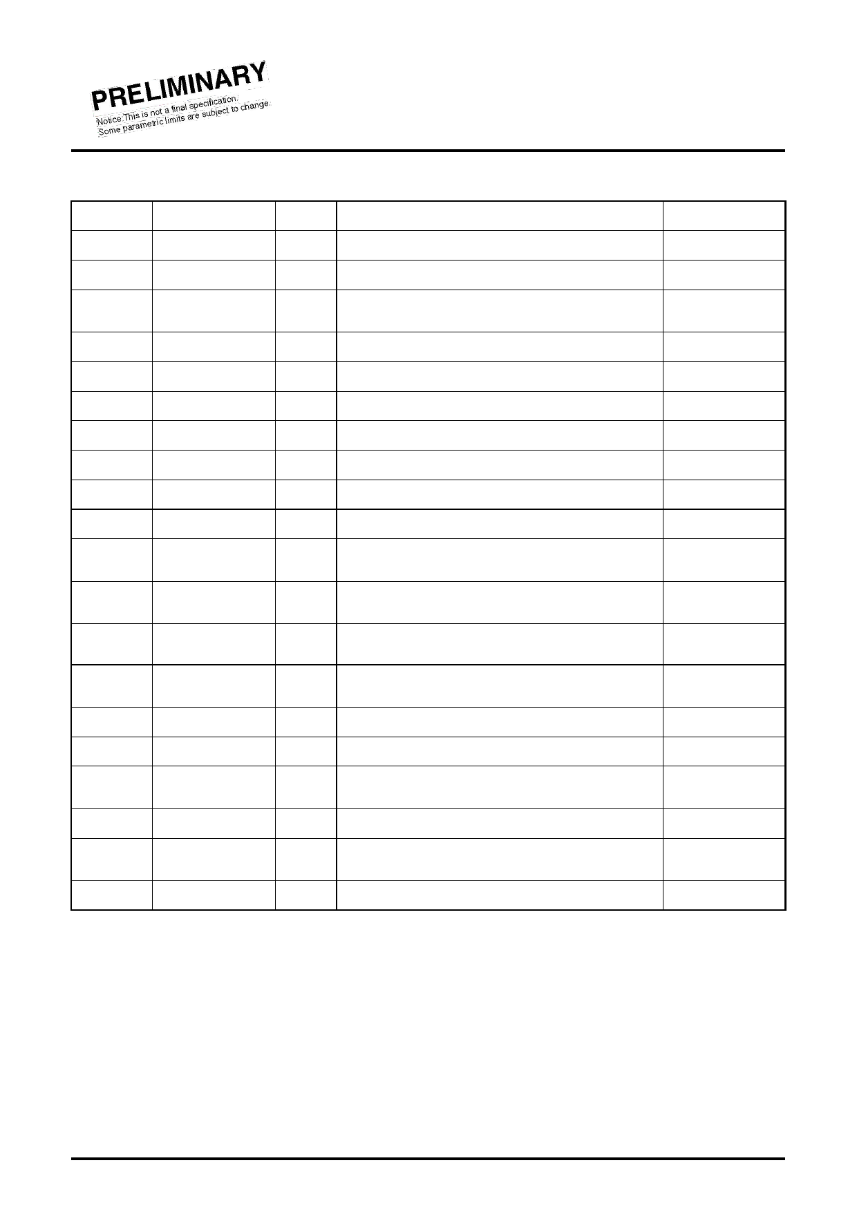
DESCRIPTION OF PIN
Pin No.
Name
1 to 10
R0 to R9
11 to 19, 21 G0 to G9
20, 34, 35 N.C.
22 to 31
32
33
36 to 38
39
40
41
B0 to B9
BLK
CEB
CLKR,G,B
DVSS
VG2
AVSS
42 to 44 IrefR,G,B
45 to 47 VGR,G,B
48, 50, 52 VG1R,G,B
49, 51, 53 VG1’R,G,B
54
AVSS
55
VZ
56, 60, 64 I OUT R,G,B
57, 61, 65 I OUT RB,GB,BB
58, 59, 62
63, 66, 67
AVDD
68
DVDD
MITSUBISHI ICs (AV COMMON)
M65530FP
TRIPLE 10-BIT VIDEO D-A CONVERTER
I/O
Function
It connects to ---
I
Digital input pin for a DAC (Red channel).
DSP LSI
I
Digital input pin for a DAC (Green channel).
DSP LSI
-
No connection.
It is grounded during actual use.
GND
I
Digital input pin for a DAC (Blue channel).
DSP LSI
I
Analog output setting during a blanking interval.
Control LSI
I
Power-down control during unused conditions.
Control LSI
I
Clock input.
DSP LSI
-
Digital ground.
GND
O
Reference voltage for a current switch.
Bypass capacitor
-
Analog ground.
GND
O
The resistor for a conversion between voltage and current is Current setting
connected to this pin.
resistor
I
A voltage input for an analog output current control.
It is connected to the VZ(pin 55) during an actual use.
Variable resistor
O
Phase compensation for a reference current source.
Phase compen.
capacitor
I
A reference voltage input for a current matrix.
It is connected to VG1 according to the application.
Phase compen.
capacitor
-
Analog ground.
GND
O
Reference voltage output.
Bypass capacitor
O
Analog output.
Output terminal
(filter)
O
Inverse analog output.
GND
-
Analog supply voltage of 5.0V.
Power supply
-
Digital supply voltage of 5.0V.
Power supply
4
Share Link: 