MAX809 View Datasheet(PDF) - Estek Electronics Co. Ltd
Part Name
Description
Manufacturer
MAX809 Datasheet PDF : 7 Pages
| |||
MAX809, MAX810
MAX809, MAX810
APPLICATIONS INFORMATION
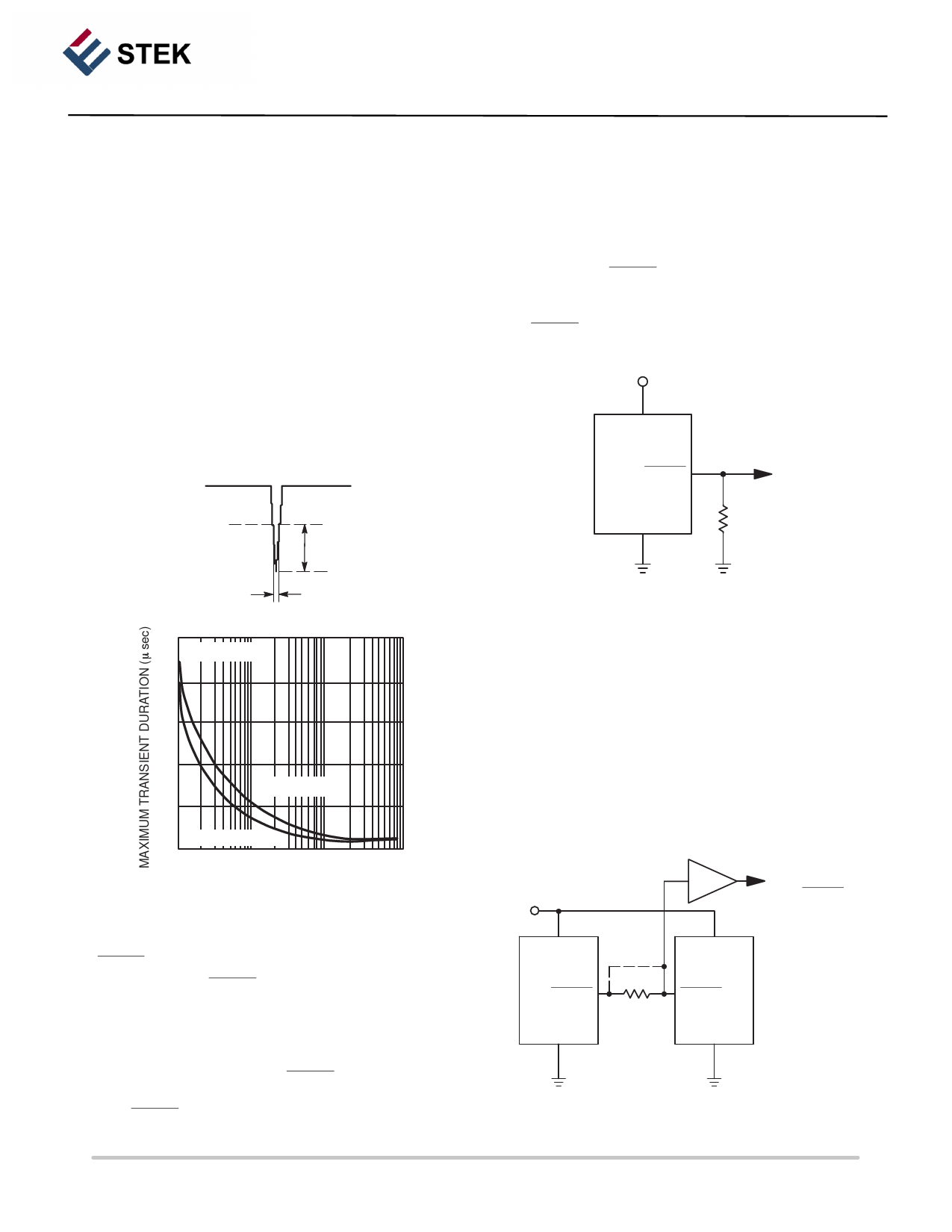
VCC Transient Rejection
The MAX809/810 provides accurate VCC monitoring and
reset timing during power–up, power–down, and
brownout/sag conditions, and rejects negative–going
transients (glitches) on the power supply line. Figure 1
shows the maximum transient duration vs. maximum
negative excursion (overdrive) for glitch rejection. Any
combination of duration and overdrive which lies under the
curve will not generate a reset signal. Combinations above
the curve are detected as a brownout or power–down.
Transient immunity can be improved by adding a capacitor
in close proximity to the VCC pin of the MAX809/810.
VCC
VTH
Overdrive
hold the output low (Figure 2). This resistor value, though
not critical, should be chosen such that it does not
W appreciably load RESET under normal operation (100k
will be suitable for most applications). Similarly, a pull–up
resistor to VCC is required for the MAX810 to ensure a valid
high RESET for VCC below 1.0V.
VCC
VCC
MAX809
RESET
GND
R1
100 k
Duration
400
TA = +25° C
320
240
160
MAX8xxL/M/J
90
0 MAX8xxR/S/T
1
10
100
1000
RESET COMPARATOR OVERDRIVE,
(VTH – VCC (mV)
Figure 1. Maximum Transient Duration vs. Overdrive
for Glitch Rejection at 25° C
RESET Signal Integrity During Power–Down
The MAX809 RESET output is valid to VCC = 1.0V.
Below this voltage the output becomes an ”open circuit” and
does not sink current. This means CMOS logic inputs to the
µP will be floating at an undetermined voltage. Most digital
systems are completely shutdown well above this voltage.
However, in situations where RESET must be maintained
valid to VCC = 0V, a pull–down resistor must be connected
from RESET to ground to discharge stray capacitances and
Figure 2. Ensuring RESET Valid to VCC = 0 V
Processors With Bidirectional I/O Pins
Some µP’s (such as Motorola 68HC11) have
bi–directional reset pins. Depending on the current drive
capability of the processor pin, an indeterminate logic level
may result if there is a logic conflict. This can be avoided
W by adding a 4.7k resistor in series with the output of the
MAX809/810 (Figure 3). If there are other components in
the system which require a reset signal, they should be
buffered so as not to load the reset line. If the other
components are required to follow the reset I/O of the µP, the
buffer should be connected as shown with the solid line.
VCC
VCC
MAX809
RESET
GND
BUFFER
BUFFERED RESET
TO OTHER SYSTEM
COMPONENTS
VCC
mP
47 k
RESET
GND
Figure 3. Interfacing to Bidirectional Reset I/O
4
Share Link: 