MAX8727 View Datasheet(PDF) - Maxim Integrated
Part Name
Description
Manufacturer
MAX8727 Datasheet PDF : 13 Pages
| |||
TFT-LCD Step-Up DC-DC Converter
ABSOLUTE MAXIMUM RATINGS
LX to GND ..............................................................-0.3V to +26V
IN, SHDN, FREQ, FB to GND ...................................-0.3V to +6V
COMP, SS to GND .........................................-0.3V to VIN + 0.3V
LX Switch Maximum Continuous RMS Current .....................2.4A
Continuous Power Dissipation (TA = +70°C)
10-Pin Thin DFN (derate 24.4mW/°C above +70°C) ....1951mW
Operating Temperature Range ...........................-40°C to +85°C
Junction Temperature ......................................................+150°C
Storage Temperature Range .............................-65°C to +160°C
Lead Temperature (soldering, 10s) .................................+300°C
Stresses beyond those listed under “Absolute Maximum Ratings” may cause permanent damage to the device. These are stress ratings only, and functional
operation of the device at these or any other conditions beyond those indicated in the operational sections of the specifications is not implied. Exposure to
absolute maximum rating conditions for extended periods may affect device reliability.
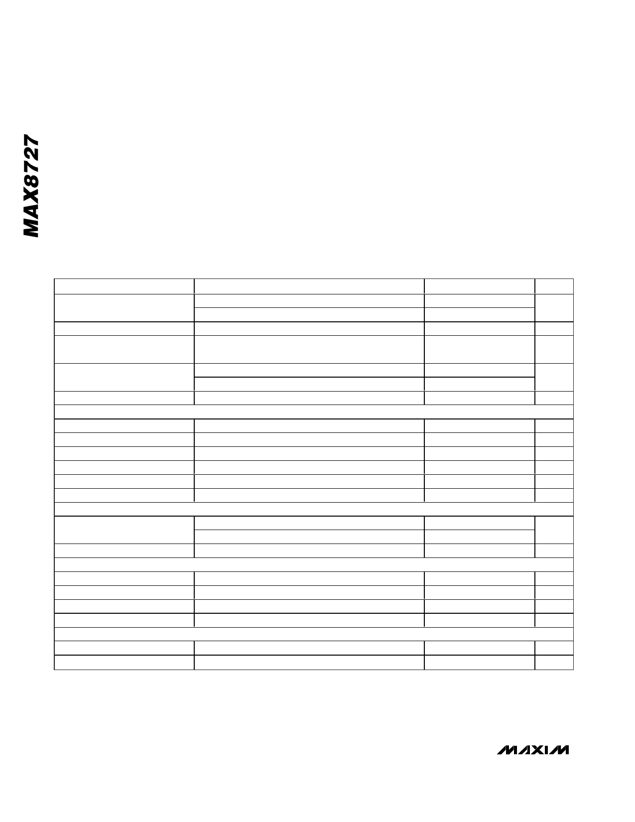
ELECTRICAL CHARACTERISTICS
(VIN = VSHDN = 3V, FREQ = GND, TA = 0°C to +85°C. Typical values are at TA = +25°C, unless otherwise noted.) (Note 1)
PARAMETER
Input Voltage Range
Output Voltage Range
IN Undervoltage-Lockout
Threshold
IN Quiescent Current
IN Shutdown Current
ERROR AMPLIFIER
FB Regulation Voltage
FB Input Bias Current
FB Line Regulation
Transconductance
Voltage Gain
Shutdown FB Input Voltage
OSCILLATOR
Frequency
Maximum Duty Cycle
n-CHANNEL MOSFET
Current Limit
On-Resistance
Leakage Current
Current-Sense Transresistance
SOFT-START
Reset Switch Resistance
Charge Current
VOUT < 18V
18V < VOUT < 24V
CONDITIONS
VIN rising, typical hysteresis is 50mV
VFB = 1.3V, not switching
VFB = 1.0V, switching
SHDN = GND
Level to produce VCOMP = 1.24V
VFB = 1.24V
Level to produce VCOMP = 1.24V, VIN = 2.6V to 5.5V
SHDN = GND
FREQ = GND
FREQ = IN
VFB = 1V, 75% duty cycle
VLX = 24V
VSS = 1.2V
MIN TYP MAX UNITS
2.6
5.5
V
4.0
5.5
24
V
2.20 2.38 2.57
V
0.225 0.440
mA
2
5
0.1
10.0
µA
1.22 1.24 1.26
V
50
125
250
nA
0.05 0.15 %/V
100
200
300
µS
700
V/V
0.05 0.10 0.15
V
540
640
740
kHz
1000 1220 1500
87
90
93
%
3.0
3.8
4.6
A
125
250
Ω
30
45
µA
0.11 0.21 0.31
V/A
100
Ω
2.5
4.5
7.5
µA
2 _______________________________________________________________________________________
Share Link: 