MC12210D View Datasheet(PDF) - LANSDALE Semiconductor Inc.
Part Name
Description
Manufacturer
MC12210D Datasheet PDF : 11 Pages
| |||
ML12210
LANSDALE Semiconductor, Inc.
PHASE CHARACTERISTICS/VCO CHARACTERISTICS
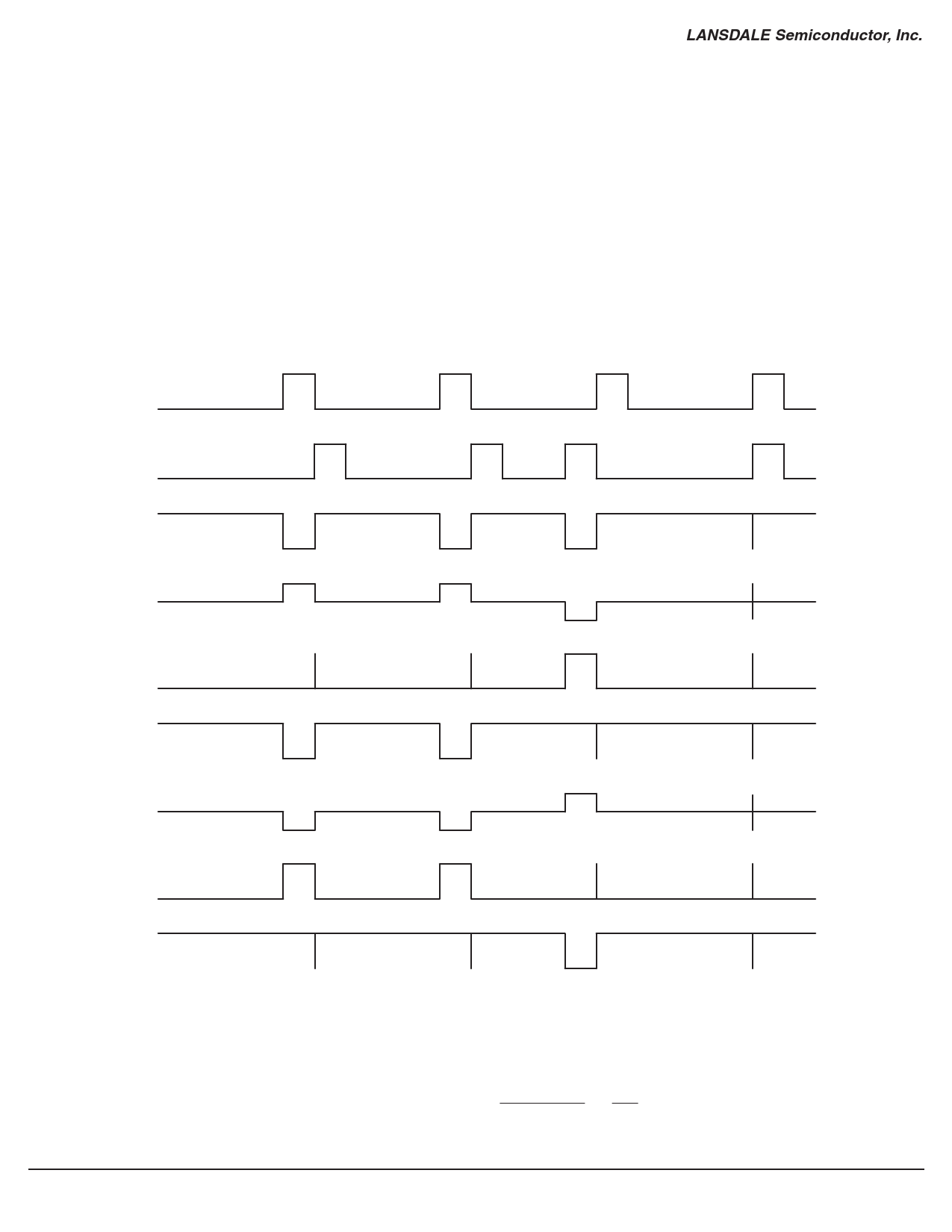
The phase comparator in the ML12210 is a high speed digital phase frequency detector circuit. The circuit determines the “lead” or “lag”
phase relationship and time difference between the leading edges of the VCO (fp) signal and the reference (fr) input. Since these edges
occur only once per cycle, the detector has a range of ±2π radians. The phase comparator outputs are standard CMOS rail–to–rail levels
(VP to GND for φP and VCC to GND for φR), designed for up to 20MHz operation into a 15pF load. These phase comparator outputs
can be used along with an external charge pump to enhance the PLL characteristics.
The operation of the phase comparator is shown in Figures 3 and 5. The phase characteristics of the phase comparator are controlled by
the FC pin. The polarity of the phase comparator outputs, φR and φP, as well as the charge pump output Do can be reversed by switching
the FC pin.
Figure 3. Phase/Frequency Detector, Internal Charge Pump and Lock Detect Waveforms
fr
fp
LD
Do (FC = H)
BISW (LE = H or Open)
φR (FC = H)
φP (FC = H)
Do (FC = L)
BISW (LE = H or Open)
φR (FC = L)
φP (FC = L)
NOTES: Do and BISW are current outputs.
Phase difference detection range: –2π to +2π
Spike difference depends on charge pump characteristics. Also, the spike is output in order to diminish dead band.
When fr > fp or fr < fp, spike might not appear depending upon charge pump characteristics.
Internal Charge Pump Gain ≈
Isource + Isink = 4mA
4π
4π
H
L
H
L
H
L
Source
Z
Sink
H
L
H
L
Source
Z
Sink
H
L
H
L
Page 6 of 11
www.lansdale.com
Issue A
Share Link: 