NT68275 View Datasheet(PDF) - Unspecified
Part Name
Description
Manufacturer
NT68275 Datasheet PDF : 38 Pages
| |||
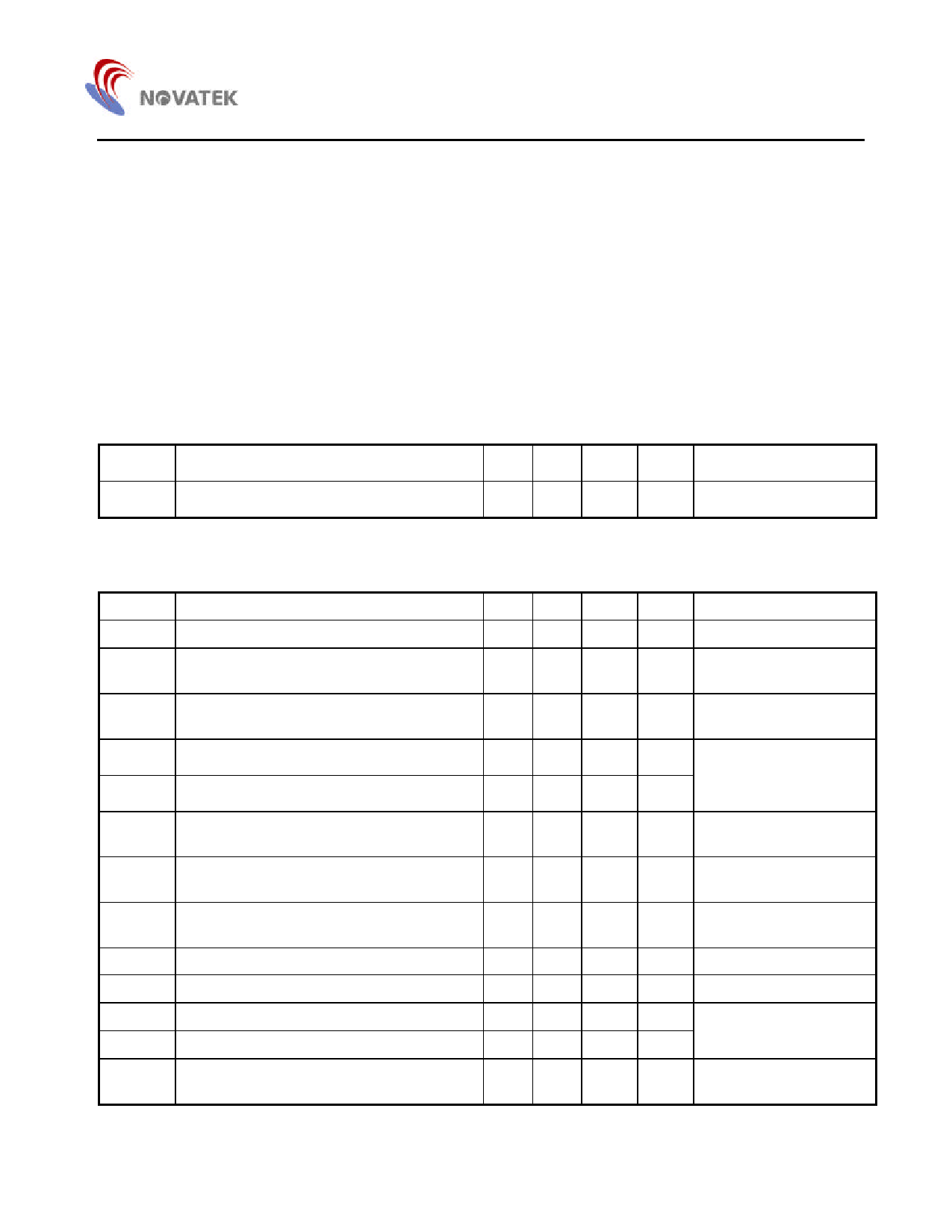
DC/AC Absolute Maximum Ratings*
Recommended Operating Conditions
VCC (measured to GND) . . . . . . . . . .. . 4.75V to 5.25V
Operating Temperature . . . . . . . . . . . . . 0 to +70 0C
NT68275
*Comments
Stresses above those listed under "Absolute
Maximum Ratings" may cause permanent damage to
this device. These are stress ratings only. Functional
operation of this device at these or any other
conditions above those indicated in the operational
sections of this specification is not implied or
intended. Exposed to the absolute maximum rating
conditions for extended periods may affect device
reliability.
Electrical Characteristics (VDD = 5V, Tamb = 25° C)
Symbol
Parameter
Min. Typ. Max. Unit
VCC Supply Voltage
4.75 5 5.25 V
Notes
DC Characteristic
Symbol
IDD
Parameter
Operating Current
VIH1 Input High Voltage
VIL1
VIH2
VIL2
Input Low Voltage
IIC Bus Input High Voltage
IIC Bus Input Low Voltage
Min. Typ. Max.
22 25
2
0.8
3
1.5
Unit
mA
V
V
V
V
Notes
No loading
VFLB, HFLB with
Schmitt Trigger Buffer
VFLB, HFLB Schmitt
Trigger Buffer
SCL, SDA
Idrive1
Isink1
Ileak
Iiicl
Vth
VSTIH
VSTIL
Iin
Driving current of R, G, B, FBKG, HFTON
output pins at 2.4V output voltage
80
Sinking current of R, G, B, FBKG, HFTON
output pins at 0.4V output voltage
20
Leakage current of R, G, B, FBKG pins at
Hi-Z state
10
IIC Bus Output Sink Current
5
Input Threshold Voltage at HFLB & VFLB 1.8 2.0 2.2
Schmitt Trigger Input High Voltage
1.7
2
Schmitt Trigger Input Low Voltage
0.8 1.1
Input Current of Hsync, Vsync, SDA, SCL
pins
-10
+10
mA
mA
uA Measured at 2.5V state
mA Viicoutl = 0.4V
V
V
Refer Figure 1
V
uA Schmitt Trigger Buffer
5
Share Link: 