VKP100MT315 View Datasheet(PDF) - C AND D TECHNOLOGIES
Part Name
Description
Manufacturer
VKP100MT315 Datasheet PDF : 6 Pages
| |||
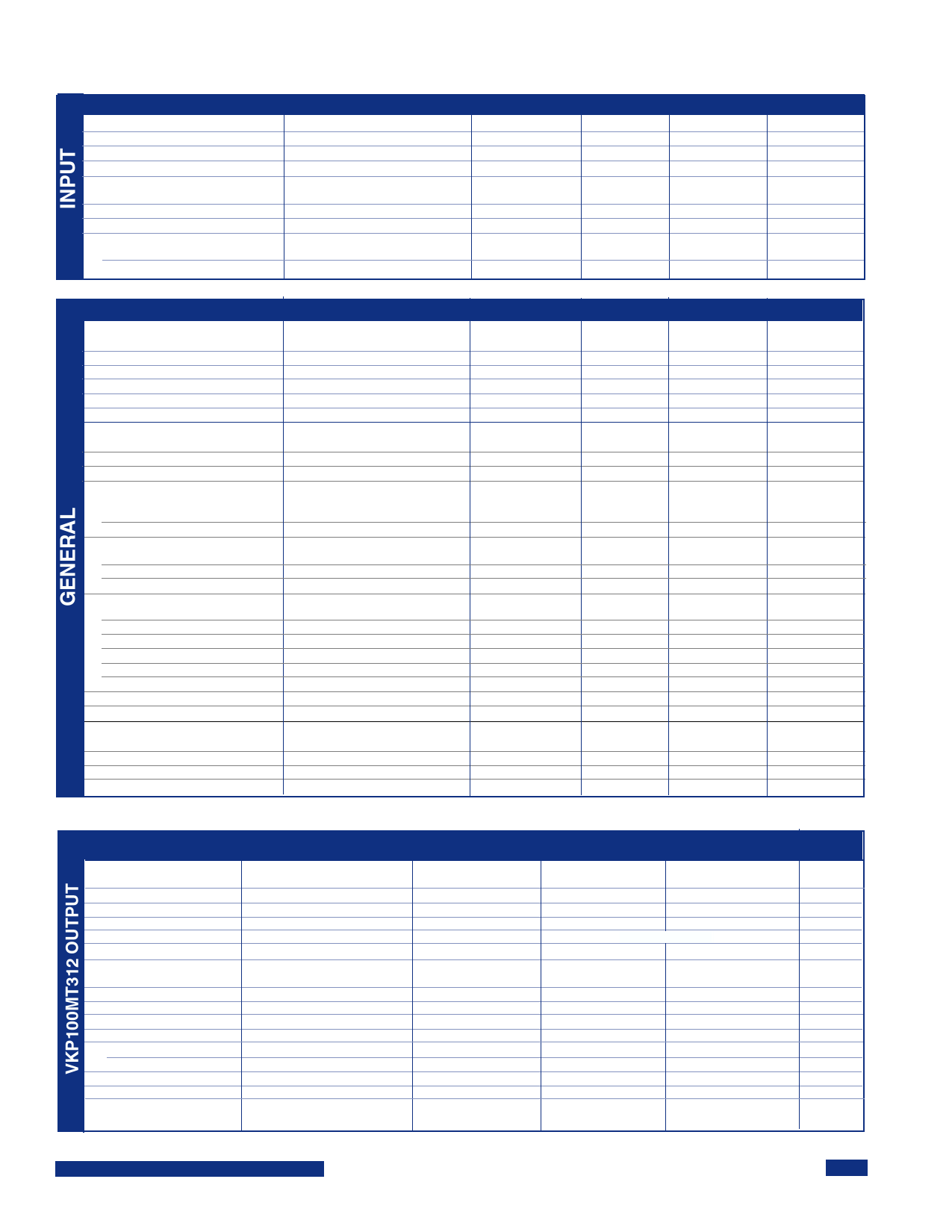
SPECIFICATIONS, ALL MODELS
Specifications are at T = +40°C nominal input voltage unless otherwise specified.
CASE
PARAMETER
CONDITIONS
MIN
Input Fusing
Voltage Range
33
Reflected Ripple Current
Peak - Peak
Input Ripple Rejection
DC to 1KHz
50
Maximum Input Current
Output Power = 100W
No Load Power Dissipation
Inrush Charge
VIN = 30V
POUT = 0, VIN, Min<VIN<VIN, Max
Quiescent Operating Current
Primary On/Off Disabled
Secondary On/Off Disabled
TYP
48
60
7.5
15
PARAMETER
ISOLATION
Input to Each Output
Input to Baseplate
Channel to Channel
Resistance, Input - Output
Capacitance, Input - Output
Leakage Current
GENERAL
Set Point Accuracy
Turn-on Time
Remote On/Off Control Inputs
Primary
Sink Current-Logic Low
Vlow
Vhigh
Secondary
Sink Current-Logic Low
Vlow
Vhigh
External Synchronization Input
Frequency
Pulse Width
Source Impedence
Input High Voltage
Input Low Voltage
Input Impedance
Switching Frequency
Weight
TEMPERATURE
Operation/Specification
Storage
Shutdown
Thermal Inpedance
CONDITIONS
Peak Test
Any Channel to Any Channel
V
ISO
=
240VAC,
60Hz
VIN = Nominal, 50% Load
Within 1% of Nominal VOUT
Open Collector/Drain
VIN = VMAX
Open Collector/Drain
Case Temperature
Case to Ambient
MIN
1500
1500
500
10
440
150
4
0
470
-40
-55
+100
TYP
2000
180
3.5
470
480
8.2
MAX
10
75
370
5
6
0.247
10
20
MAX
1
5
7
0.8
Open Collector
100
0.4
Open Collector
520
320
47
5
1
490
3 (85)
+100
+125
+115
UNITS
A
VDC
mA
dB
A
W
mC
mA
mA
UNITS
VDC
VDC
VDC
MΩ
pF
µA, rms
%
mSec
mA
V
µA
V
KHz
nSec
Ω
V
V
Ω
KHz
oz (g)
°C
°C
°C
°C/W
PARAMETER
Output Power
Set Point Voltage
Output Current, IOUT
Output Ripple, p-p
Output Adjust Range
Output Temperature Drift
Line Regulation
Load Regulation
CONDITIONS
Total Combined O/P Power =
100 Watts Max
IO Nom
DC to 20MHz*
*
VIN, Min≤VIN≤VIN, Max
IO = IO, Nom
Min Load to Rated Load
V1
V2
Min Nom Max Min Nom Max
Min
V3
Nom
Max
UNITS
50 100
25
50
25
50
3.3
12.2
12.2
0.5
15 30.0
0
2.1
4.2
0
2.1 4.2
100 200
150 500
150 500
3.15
3.80
Dependent on V1
.02 .05
.02
.05
.02 .05
W
V
A
mV
V
%/°C
0.05 0.10
1.0
2.0
1.0 2.0
%
0.50 1.00 See Regulation Curves See Regulation Curves
%
Current Limit Inception
Short-Circuit Current
Transient Response
Peak Deviation
Settling Time
Overvoltage Limit
Efficiency
Other Outputs Min Load
50 to 100% Load Step
VOUT, 1% of VOUT, Nom
4.2
IOUT1=15A, (IOUT2+IOUT3)= 4.2A
85
F.L. VIN=Nominal
* See Application Notes available on the web at www.cdpowerelectronics.com
38
30
38
150 250
35
50
5.0
86
Product: www.cdpowerelectronics.com
VKP100xT REV D 12/2001
6.0
5.0
6.0
6.0
5.0 6.0
A
A
mV
µSec
V
%
2
Share Link: 