VN920DSP View Datasheet(PDF) - STMicroelectronics
Part Name
Description
Manufacturer
VN920DSP Datasheet PDF : 19 Pages
| |||
VN920DSP
ELECTRICAL CHARACTERISTICS
(8V<VCC<36V; -40°C<Tj<150°C unless otherwise specified)
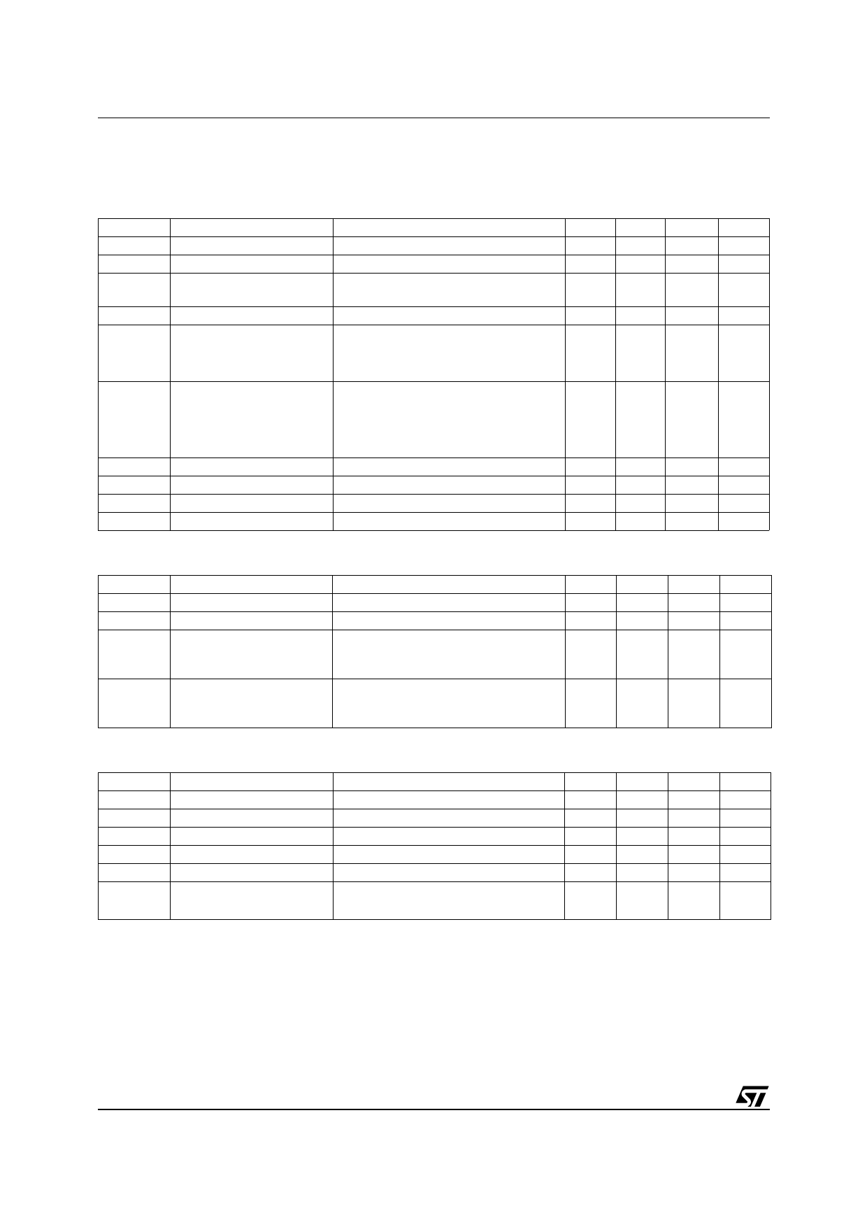
Table 5. Power
Symbol
Parameter
Test Conditions
Min Typ Max Unit
VCC Operating Supply Voltage
5.5
13
36
V
VUSD Undervoltage Shut-down
3
4
5.5
V
VUSDhyst
Undervoltage Shut-down
hysteresis
0.5
V
VOV Overvoltage Shut-down
36
V
IOUT=10A; Tj=25°C
16
mΩ
RON On State Resistance
IOUT=10A
30
mΩ
IOUT=3A; VCC=6V
Off State; VCC=13V; VIN=VOUT=0V
50
mΩ
10
25
µA
IS
Supply Current
Off State; VCC=13V; VIN=VOUT=0V;
Tj=25°C
10
20
µA
On State; VCC=13V; VIN=5V; IOUT=0A
5
mA
IL(off1) Off State Output Current VIN=VOUT=0V
0
IL(off2) Off State Output Current VIN=0V; VOUT=3.5V
-75
IL(off3) Off State Output Current VIN=VOUT=0V; VCC=13V; Tj =125°C
IL(off4) Off State Output Current VIN=VOUT=0V; VCC=13V; Tj =25°C
50
µA
0
µA
5
µA
3
µA
Table 6. Switching (VCC=13V)
Symbol
td(on)
td(off)
Parameter
Turn-on Delay Time
Turn-off Delay Time
dVOUT/
dt(on)
Turn-on Voltage Slope
dVOUT/
dt(off)
Turn-off Voltage Slope
Test Conditions
RL=1.3Ω
RL=1.3Ω
RL=1.3Ω
RL=1.3Ω
Min Typ Max
50
50
See
relative
diagram
See
relative
diagram
Unit
µs
µs
V/µs
V/µs
Table 7. Input Pin
Symbol
VIL
IIL
VIH
IIH
VI(hyst)
Parameter
Input Low Level
Low Level Input Current
Input High Level
High Level Input Current
Input Hysteresis Voltage
VICL Input Clamp Voltage
Test Conditions
VIN=1.25V
VIN=3.25V
IIN=1mA
IIN=-1mA
Min Typ Max Unit
1.25
V
1
µA
3.25
V
10
µA
0.5
V
6
6.8
8
V
-0.7
V
4/19
Share Link: 