ZXCL300 View Datasheet(PDF) - Diodes Incorporated.
Part Name
Description
Manufacturer
ZXCL300 Datasheet PDF : 14 Pages
| |||
ZXCL SERIES
Applications information
Enable control
A TTL compatible input is provided to allow the
regulator to be shut down. A low voltage on the
Enable pin puts the device into shutdown mode.
In this mode the regulator circuit is switched off
and the quiescent current reduces to virtually
zero (typically less than 10nA) for input voltages
above the minimum operating threshold of the
device. A high voltage on the Enable pin ensures
normal operation.
The Enable pin can be connected to VIN or
driven from an independent source of up to 10V
maximum. (e.g. CMOS logic) for normal
operation. There is no clamp diode from the
Enable pin to VIN, so the VIN pin may be at any
voltage within its operating range irrespective
of the voltage on the Enable pin. However input
voltage rise time should be kept below 5ms to
ensure consistent start-up response.
Current Limit
The ZXCL devices include a current limit circuit
which restricts the maximum output current
flow to typically 230mA. Practically the range of
over-current should be considered as minimum
160mA to maximum 800mA. The device’s
robust design means that an output short circuit
to any voltage between ground and VOUT can be
tolerated for an indefinite period.
Thermal Overload
Thermal overload protection is included on
chip. When the device junction temperature
exceeds a minimum 125°C the device will shut
down. The sense circuit will re-activate the
output as the device cools. It will then cycle until
the overload is removed. The thermal overload
protection will be activated when high load
currents or high input to output voltage
differentials cause excess dissipation in the
device.
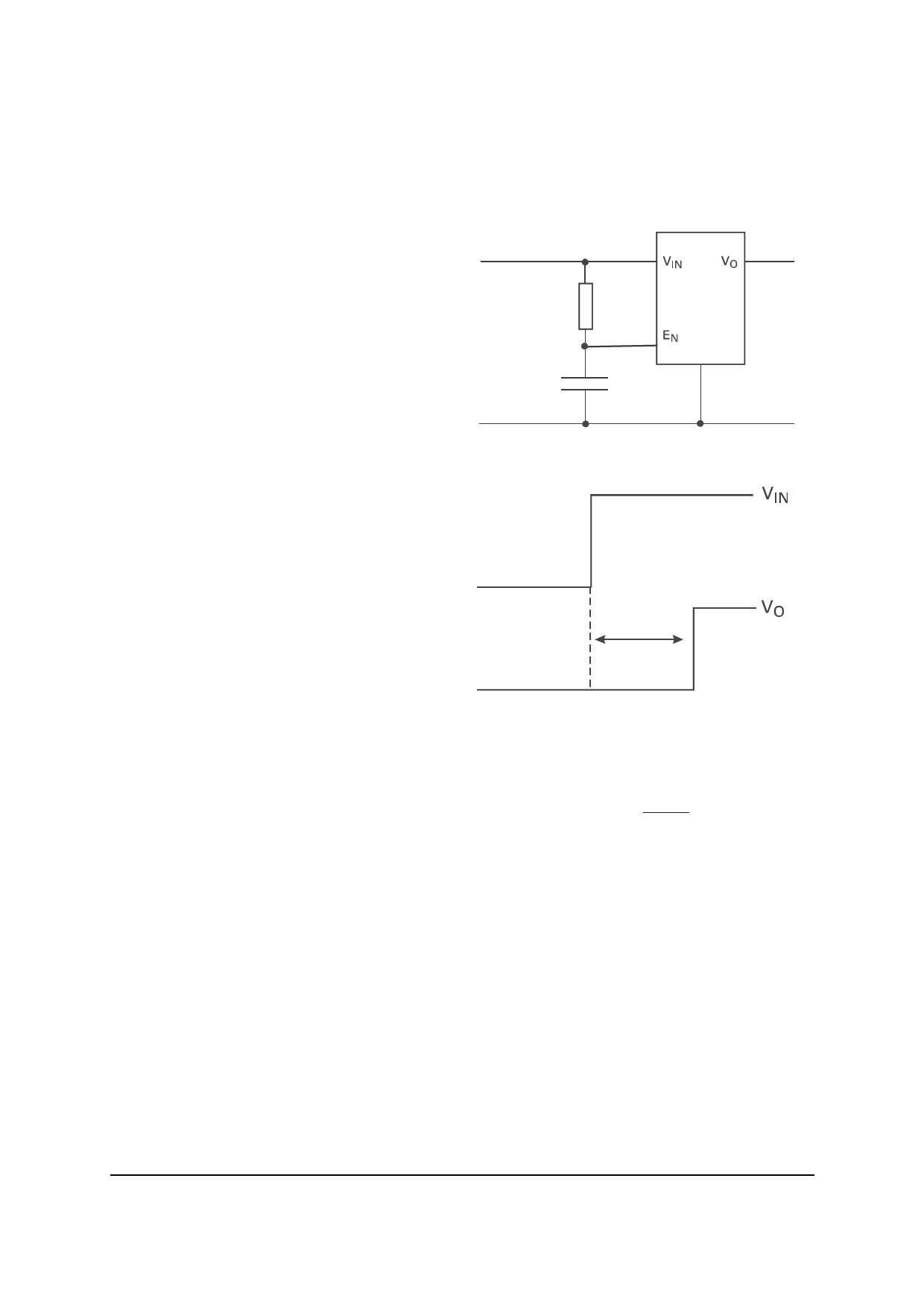
Start up delay
A small amount of hysteresis is provided on the
Enable pin to ensure clean switching. This
feature can be used to introduce a start up delay
if required. Addition of a simple RC network on
the Enable pin provides this function. The
following diagram illustrates this circuit
connection. The equation provided enables
calculation of the delay period.
R
C
Figure 1 Circuit Connection
Td
Figure 2 Start up delay (Td)
Td(NOM)
=
⎛
RCIn⎜
⎝
VIN
VIN − 1.5
⎞
⎟
⎠
Calculation of start up delay as above
Issue 8 - October 2007
9
© Zetex Semiconductors plc 2007
www.zetex.com
Share Link: 