IS457 View Datasheet(PDF) - Sharp Electronics
Part Name
Description
Manufacturer
IS457 Datasheet PDF : 4 Pages
| |||
IS457
s Electro-optical Characteristics
Parameter
High level output voltage
Low level output voltage
High level supply current
Low level supply current
Ro terminal offset voltage
*4"High →Low" threshold illuminance 1
*4"High →Low" threshold illuminance 2
"High→Low" threshold incident light intensity
"High→Low" propagation delay time
Response time
"Low →High" propagation delay time
Rise time
Fall time
Symbol
I OH
V OL
I CCH
ICCL
I OSRO
E VHL1
E VHL2
P IHL
t PHL
t PLH
tr
tf
Conditions
RO=51kΩ , E v=0 lx
IOL=40mA, E V=1 000 lx
RO=51kΩ , EV=0 lx
RO=51kΩ , EV=1 000 lx
R O=5.1kΩ
R O=51kΩ
R O=5.1kΩ
RO=5.1kΩ , λ =780nm
CL=15pF, Duty ratio=1:1
P I=0.2mW, λ =780nm
RO=5.1kΩ , R L=510Ω
*4 E VHL1 , E VHL2 : Illuminance by CIE standard light source A (tungsten lamp) to bring about change from "High" to "Low"
MIN.
-
-
-
-
-
250
-
-
-
-
-
-
(VCC = 5V, Ta = 25˚C)
TYP. MAX. Unit
-
100
µA
0.35 0.52
V
3.0
6.5
mA
5.8
8.6
mA
8
15
µA
360 470
lx
4 500
-
lx
100
-
µW
300 500
ns
300 500
ns
100 500
ns
50
200
ns
s Recommended Operating Conditions
Parameter
Operating supply voltage
Operating temperature
Incident light intensity ( λ=780 nm)
Gain resistance
Symbol MIN. MAX. Unit
V cc
4.5
5.5
V
T opr
0
60
˚C
PI
-
2.5
mW
RO
0.39
5.1
kΩ
In order to stabilize power supply line, connect a by-pass capacitor of 0.1 µF between Vcc and GND
at a position within 1 cm from the lead.
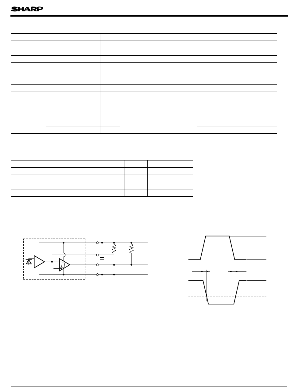
s Test Circuit for Response Time
Vcc
5V
Ro
5.1kΩ 510Ω
0.1 µ F
Vo
Vo
Vref
GND
CL
GND
Notes 1. CL includes the probe-to-line capacitance.
2. Add a by-pass capacitor of 0.1µF at a position
within 1 cm from the Vcc-GND terminal.
PI
t PHL
VO
0.2mW
0.1mW
t PLH
0mW
5.0V
1.5V
Share Link: 