CP05C(2007) View Datasheet(PDF) - Protek Devices
Part Name
Description
Manufacturer
CP05C Datasheet PDF : 5 Pages
| |||
APPLICATION NOTE
CP05
thru
CP24C
The CP Series are TVS arrays designed to protect I/O or data lines from the damaging effects of ESD or EFT. This product series provides both
unidirectional and bidirectional protection, with a surge capability of 200 Watts PPP per line for an 8/20µs waveform and ESD protection > 25 kilovolts.
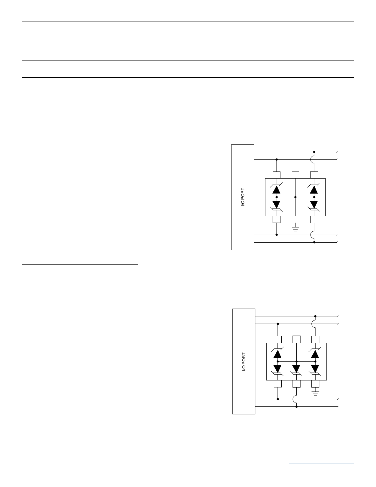
UNIDIRECTIONAL COMMON-MODE CONFIGURATION (Figure 1)
The CP Series provides up to four (4) lines of protection in a common-mode configuration as depicted in Figure 1.
Circuit connectivity is as follows:
✔ Line 1 is connected to Pin 1.
✔ Line 2 is connected to Pin 3.
✔ Line 3 is connected to Pin 4.
✔ Line 4 is connected to Pin 6.
✔ Pin 5 is connected to ground.
✔ Pin 2 is not connected.
BIDIRECTIONAL COMMON-MODE CONFIGURATION (Figure 2)
Figure 1 - Unidirectional Configuration
Common-Mode I/O Port Protection
LINE 1
LINE 2
3
2
1
The CPxxC Series provides up to four (4) lines of protection in a common-mode
configuration as depicted in Figure 2.
Circuit connectivity is as follows:
✔ Line 1 is connected to Pin 1.
✔ Line 2 is connected to Pin 3.
✔ Line 3 is connected to Pin 4.
✔ Line 4 is connected to Pin 5.
✔ Pin 6 is connected to ground.
✔ Pin 2 is not connected.
4
5
6
LINE 3
LINE 4
CIRCUIT BOARD LAYOUT RECOMMENDATIONS
Circuit board layout is critical for Electromagnetic
Compatibility (EMC) protection. The following
guidelines are recommended:
✔ The protection device should be placed near the
input terminals or connectors, the device will
divert the transient current immediately before it
can be coupled into the nearby traces.
✔ The path length between the TVS device and
the protected line should be minimized.
✔ All conductive loops including power and ground
loops should be minimized.
✔ The transient current return path to ground
should be kept as short as possible to reduce
parasitic inductance.
✔ Ground planes should be used whenever
possible. For multilayer PCBs, use ground vias.
Figure 2 - Bidirectional Configuration
Common-Mode I/O Port Protection
LINE 1
LINE 2
3
2
1
4
5
6
LINE 3
LINE 4
05133.R8 2/07
4
www.protekdevices.com
Share Link: 