CA3273 View Datasheet(PDF) - Intersil
Part Name
Description
Manufacturer
CA3273 Datasheet PDF : 4 Pages
| |||
Specifications CA3273
Absolute Maximum Ratings
Thermal Information
Fault Max, Supply Voltage, VCC . . . . . . . . . . . . . . . . . . . . . . . . . 40V
Maximum Operating VCC:
At IO = 400mA (-40oC to +85oC Ambient) . . . . . . . . . . . . . . 16V
At IO = 600mA (-40oC to +25oC Ambient) . . . . . . . . . . . . . . 24V
Max. Positive Output Peak Pulse, VSW Open . . . . . . . . . .VCC+12V
Max. Operating Output Load Current . . . . . . . . . . . . . . . . . . 600mA
Short Circuit Load Current, ISC . . . . . . . . . . . . . . . . Internal Limiting
Reverse Battery . . . . . . . . . . . . . . . . . . . . . . . . . . . . . . . . . . . . -13V
Thermal Resistance
θJA
Plastic SIP Package . . . . . . . . . . . . . . . . . . . . . . . . . . . +70oC/W
Maximum Power Dissipation, PD
At +25oC Ambient, TA (Note 1). . . . . . . . . . . . . . . . . . . . . . . 1.8W
Derate above +25oC (No Heat Sink) . . . . . . . . . . . . . 14.3mW/oC
Maximum Junction Temperature, TJ (Note 2) . . . . . . . . . . . . 150oC
Ambient Operating Temperature Range . . . . . . . . . -40oC to +85oC
Storage Temperature Range. . . . . . . . . . . . . . . . . . -40oC to +150oC
Lead Temperature (Soldering 10s max) . . . . . . . . . . . . . . . . +265oC
CAUTION: Stresses above those listed in “Absolute Maximum Ratings” may cause permanent damage to the device. This is a stress only rating and operation
of the device at these or any other conditions above those indicated in the operational sections of this specification is not implied.
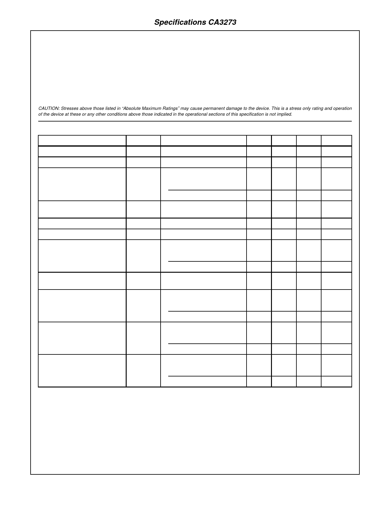
Electrical Specifications TA = -40oC to +85oC, Unless Otherwise Noted, See Block Diagram for Test Pin Reference
PARAMETERS
SYMBOL
TEST CONDITIONS
MIN
TYP
MAX
UNITS
Operating Voltage Range
VCC
VCC Reference to VSW
4
-
24
V
Saturation Voltage(VCC - VO)
VSAT
IO = -400mA, VSW = 0V, VCC = 16V
-
-
0.5
V
Operating Load
RL
VSW = 0V (Switch ON)
TA = +85oC, VCC = 16V
40
-
-
Ω
TA = +25oC,VCC = 24V
40
Ω
Over-Voltage Shutdown Threshold
VCC(THD) VSW = 0V, RL = 1kΩ, Increase VCC,
25
33
40
V
(VO goes low)
Over-Current Limiting
Over-Temperature Limiting
IO(LIM)
VCC =16V, VSW = 1V (Switch ON)
-
-
1.2
A
TLIM
-
150
-
oC
Control Current, Switch ON
ISW
VCC =16V, VSW = 0V
IO = 0mA
-
-15
-
mA
IO = -400mA
-
-22
-
mA
Control Current, Max. Load,
Switch ON
VCC = 24V, VSW = 0V,
IO = -600mA
-
-33
-
mA
Max. Control Current,High and
Low VCC
ISW(MAX)
RL = 40Ω, VSW = 1V
VCC = 24V
-50
-
-
mA
VCC = 7V
-50
-
-
mA
Min. Control Current, No Load,
Switch OFF
ISW(NL)
VO = Open, (Switch OFF)
VCC = 24V,VSW = 23V
-200
-
+50
µA
VCC = 7V, VSW = 6V
-200
-
+50
µA
Output Current Leakage
IO(LEAK)
VO = 0V, VCC = 16V, (Switch OFF)
VSW =16V
-100
-
+100
µA
VSW =15V
-100
-
+100
µA
NOTES:
1. The calculation for dissipation and junction temperature rise due to dissipation is: PD = (VCC - VO)x I O + VCC x ISW and
TJ = TA + PD x θJA where TJ is device junction temperature, TA is ambient temperature and θJA is the junction-to-ambient
thermal resistance.
2. Thermal limiting occurs at +150oC on the chip.
3-4
Share Link: 