INT201PF1 View Datasheet(PDF) - Power Integrations, Inc
Part Name
Description
Manufacturer
INT201PF1 Datasheet PDF : 12 Pages
| |||
INT201
Pin Functional Description
Pin 1:
No connection.
Pin 2:
No connection.
Pin 4:
Level shift input HSD 2 works in
conjunction with HSD 1 to provide
interface from the low side control logic
and to give noise immunity.
Pin 3:
Level shift input HSD 1 works in
conjunction with HSD 2 to provide
interface from the low side control logic
and to give noise immunity.
Pin 5:
SOURCE connection. Analog reference
point for the circuit, normally connected
to the source of the high side MOSFET.
Pin 6:
HS OUT is the output of the MOSFET
driver for the high side.
Pin 7:
No connection.
Pin 8:
V supplies power to the control logic
DDH
and output driver.
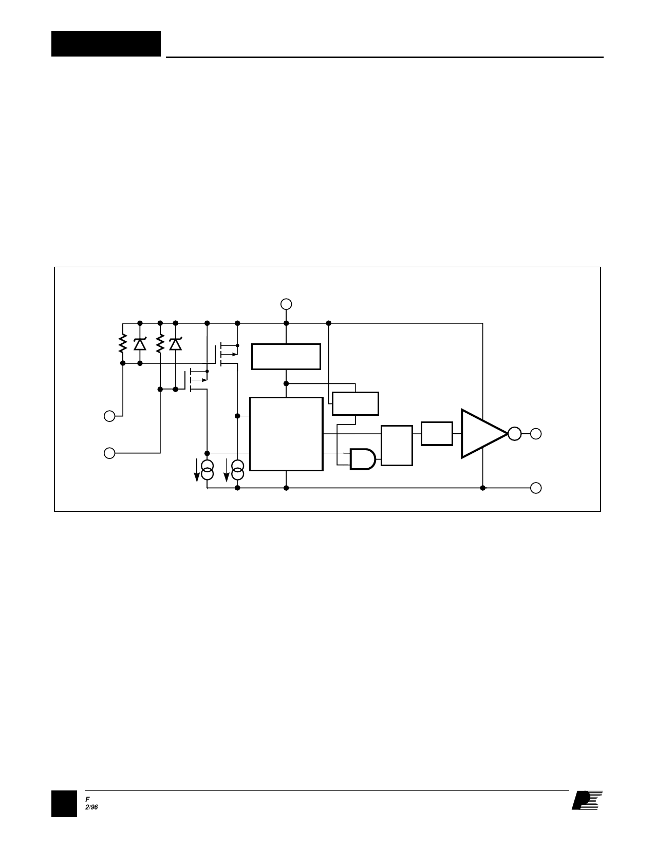
VDDH
LINEAR
REGULATOR
HSD1
HSD2
UV
LOCKOUT
DISCRIMINATOR
S Q DELAY
R
HS OUT
Figure 3. Functional Block Diagram of the INT201.
SOURCE
PI-514B-021792
INT201 Functional Description
5 V Regulator
The 5 V linear regulator circuit provides
the supply voltage for the noise rejection
circuitry and control logic. This allows
the logic section and the driver circuitry
to be directly compatible with 5 V CMOS
logic without the need of an external 5 V
supply.
Undervoltage Lockout
The undervoltage lockout circuit disables
the HS OUT pin whenever the VDDH
power supply falls below 9.0 V, and
maintains this condition until the V
DDH
power supply rises above 9.35 V. This
guarantees that the high side MOSFET
will be off during power-up or fault
conditions.
Noise Immunization Circuit
This circuit provides noise immunity by
combining a sampling circuit with a
flip-flop to turn on and off the driver
only when required to and not when
there is noise on the HSD inputs.
Driver
The CMOS driver circuit provides drive
power to the gate of the MOSFET used
on the high side of the half bridge circuit.
The driver consists of a CMOS buffer
capable of driving external transistors at
up to 15 V. The SOURCE pin is
connected to the source of the external
MOSFET to establish a reference for the
gate voltage.
2F
2/96
Share Link: 