MC33091AD View Datasheet(PDF) - Motorola => Freescale
Part Name
Description
Manufacturer
MC33091AD Datasheet PDF : 16 Pages
| |||
MC33091A
IQ is an internal current source parameter of the
MC33091A that has a nominal value of 100 µA and RX is the
external resistor in series with the drain of the TMOS device
that establishes the value of the voltage to current
proportionality constant. Since the parallel combination of RT
and CT appear at the timer pin (VT), the timer pin voltage, VT,
can be written as:
VT(t) = ISQRT[1–e–t/(RTCT)]
(2)
With the Input (Pin 7) in a logic high state and no
overcurrent condition exists, the TMOS device will be in the
“on” state. If the TMOS device experiences an overcurrent
condition, ISQ flowing through RT will increase causing CT to
charge up, in turn causing the timer voltage, VT, to exceed the
threshold, VTH, of the upper comparator. This sets the latch
causing the Q output of the latch to go high (and the Q output
to go low), causing the TMOS gate and Fault output (Pin 6) to
be pulled low, disabling the TMOS device. Both the current
squaring circuit (ISQ) and the charge pump are disabled
whenever the Q output of the latch goes low. Using Equation
2, the fault time response for an overcurrent condition can be
written as:
t = –RTCT ln(1–VTH/ISQRT)
(3)
Using Equation 1 and substituting for ISQ in Equation 3:
t = –RTCT ln[1–(VTHRX2IQ)/(VDS2RT)]
(4)
When the timer current (ISQ) is disabled, the attained VTH
voltage at Pin 8 decays according to the RTCT time constant
until the VTL threshold of the lower comparator is reached.
At this point the latch is reset and the TMOS gate, charge
pump and the current squaring circuit are again enabled,
again turning on the TMOS device. The MC33091A will
repeatedly duty cycle the TMOS gate in this manner so long
as the overcurrent condition exists and the input control
signal remains in a high logic state. The Fault output (Pin 6)
will likewise duty cycle.
Consider the case where in Equation 4 the term
(VTHRX2IQ) / (VDS2RT) ≥ 1 such that the time period is
undefined. Solving for VDS for this case yields the minimum
drain to source voltage necessary which will not allow VT to
charge to the VTH threshold of the upper comparator. In other
words, whenever the TMOS on–time period is infinite, no
TMOS overcurrent condition exists. The minimum drain to
source voltage required for uninterrupted continuous TMOS
operation is:
VDS(min) = [(VTHRX2IQ)/RT]1/2 = (VTH/KRT)1/2 (5)
Under normal operating steady state TMOS “on”
conditions; the values chosen for RX and RT should be such
that the upper comparator threshold voltage is never
reached. This insures the TMOS device will always be in
operation so long as the VDS(min) is not exceeded.
The minimum time required for the capacitor CT to charge
up to upper comparator threshold voltage occurs when the
TMOS device experiences maximum current (Imax). This will
occur when the load, and in turn the source, are shorted to
ground resulting in the full battery voltage (VS) to appear
directly across the TMOS device. This condition causes
maximum ISQ current to be produced by the current squaring
circuit. The maximum ISQ current experienced is:
ISQ(max) = KVS2 = (VS/RX)2/IQ
(6)
An expression for the minimum time–out is obtained by
substituting IQ of Equation 6 into Equation 3:
t(min) = –RTCT ln[1–VTH/(ISQ(max)RT)]
(7)
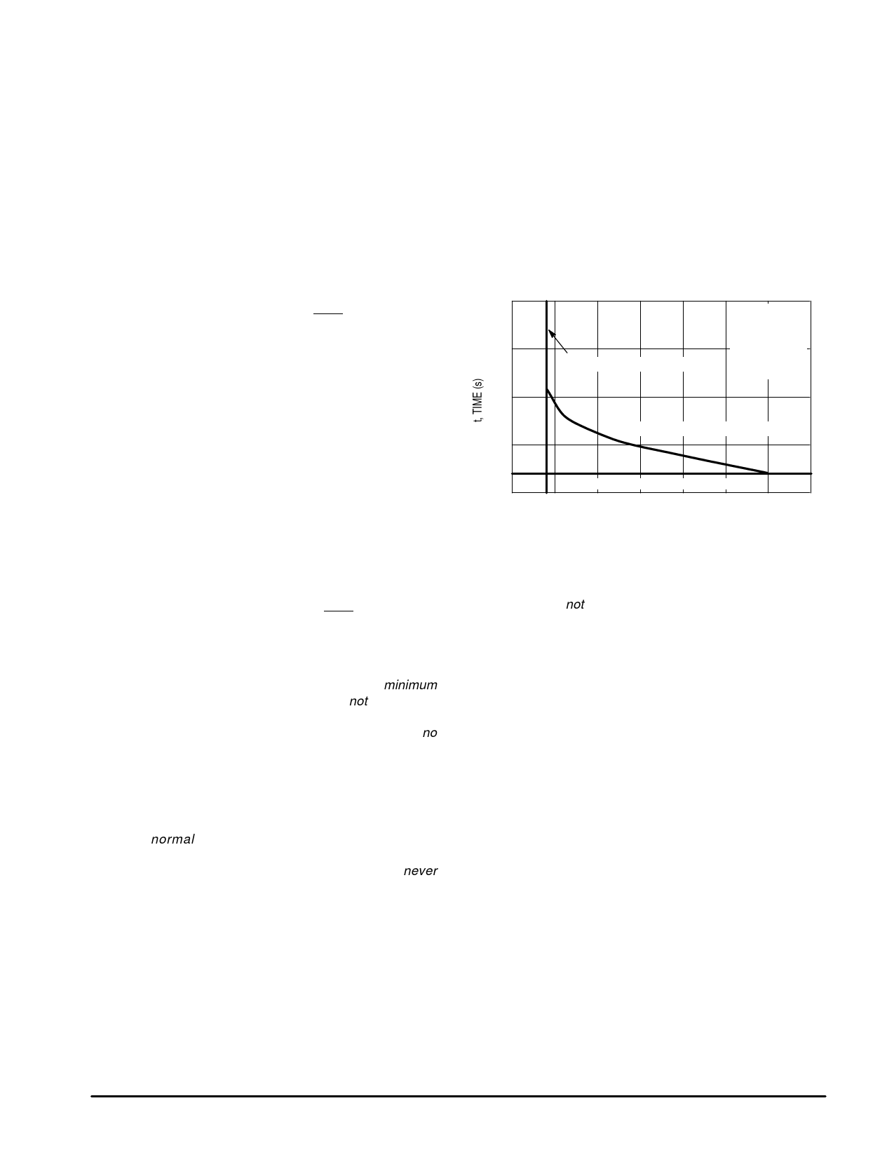
Equation 4 is shown graphically along with the asymptotic
limits imposed by Equations 5 and 7 in Figure 29.
Figure 29. Theoretical Fault Time versus VDS
100
RX = 75 k
RT = 200 k
CT = 0.02 µF
10–1
VTH = 4.6 V
VDS(min) = [(VTHRX2IQ) / RT]1/2
IQ = 100 mA
I(max) = Select
10–2
t = –RTCT In(1 – VTHRX2IQ / VDS2RT)
10–3
10–4
t(min) = –RTCT In(1 – VTH / I(max)RT)
2.0 4.0
6.0 8.0
10
12
14
16
VDS, DRAIN–TO–SOURCE VOLTAGE (V)
When driving incandescent lamp loads, the minimum timer
time–out (time required for the VT voltage to reach VTH
threshold of the upper comparator) should be set long
enough so as to not allow the in–rush current of incandescent
lamp to cause a false trigger, yet short enough to afford the
TMOS device survival protection against direct shorts under
worst case supply and temperature conditions.
TMOS Driver Power Dissipation
Under load short conditions, the MC33091A will duty cycle
the TMOS gate. The power dissipation in this mode can be
significant. For this reason proper heatsinking of the TMOS
device is essential as is the selection of compatible external
components so as to protect the TMOS device from
destruction. In most cases, the heatsink required to handle
the TMOS power dissipation under normal operating
conditions will be adequate to insure the device survives a
short circuit for an indefinite time under worst case conditions.
The MC33091A can protect the TMOS device under a
direct load short condition. If the source voltage is less than
about 1.5 V above ground, which will normally be the case in
the event of a dead short, the MC33091A will clamp the gate
to source voltage at 7.0 V. This action will limit the TMOS
current and power dissipated under a direct load short
condition.
10
MOTOROLA ANALOG IC DEVICE DATA
Share Link: 