MC33091AD View Datasheet(PDF) - Motorola => Freescale
Part Name
Description
Manufacturer
MC33091AD Datasheet PDF : 16 Pages
| |||
MC33091A
The data sheet for the particular TMOS device being used
will normally reveal the current value, IDS(max), to be
expected under a dead short condition. TMOS data sheets
normally depict graphs of drain current versus drain to source
voltage for various gate to source voltages from which the
drain current at 7.0 V VGS, IDS(max), can reasonably be
approximated. Using this information, the peak TMOS power
dissipation under a dead short condition is approximated
to be:
PD(peak) = VS(max)IDS(max)
(8)
The average power is equal to the peak power dissipation
multiplied by the duty cycle (DC):
PD(avg) = PD(peak)DC
(9)
As long as the average power, in Equation 9, is less than
the maximum power dissipation of the TMOS device under
normal conditions, the short circuit protection scheme of the
MC33091A will adequately protect the TMOS device. The
duty cycle at which the MC33091A controls the gate can be
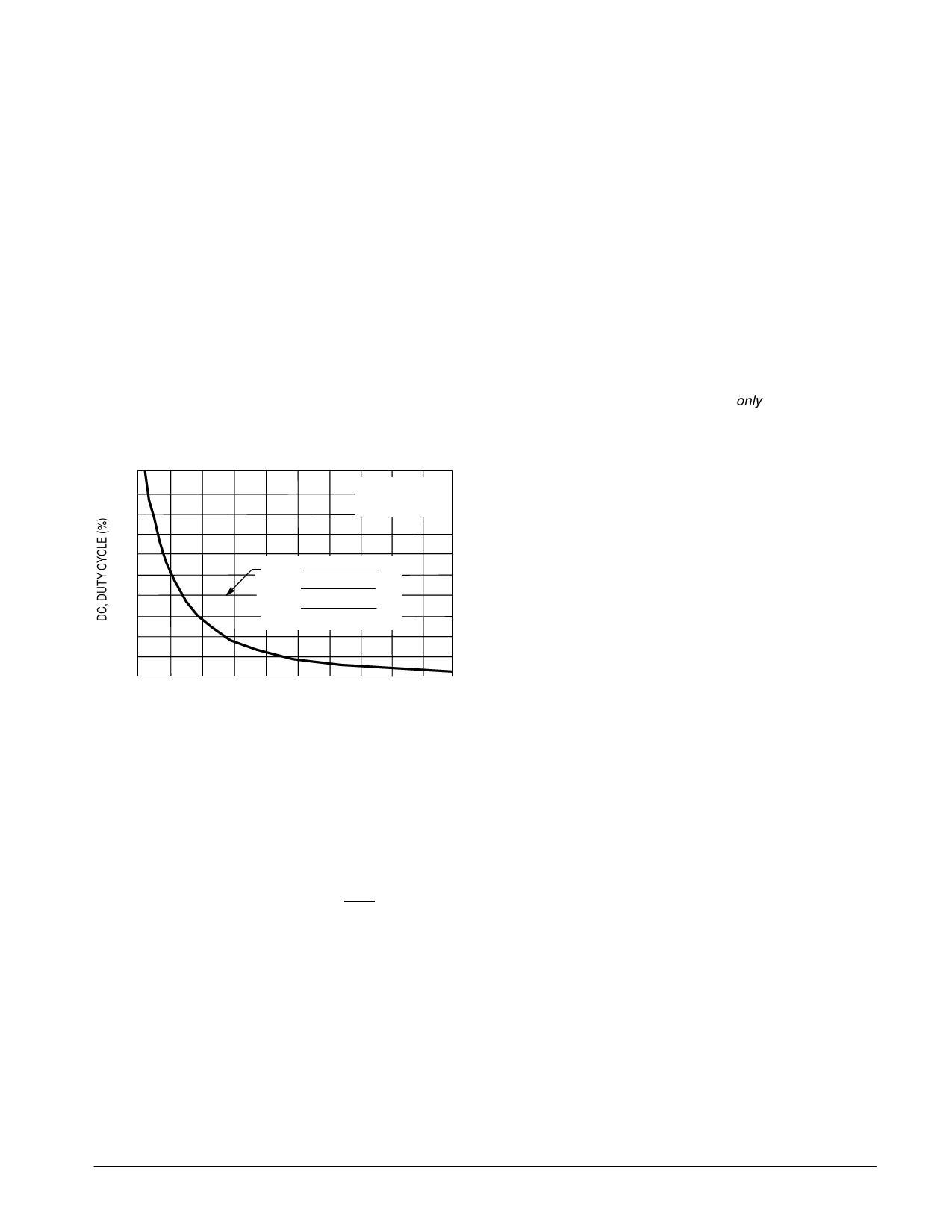
determined by using Figure 30.
Figure 30. MC33091A Duty Cycle
versus VDS / VDS(min)
10
VTH = 4.6 V
VTL = 0.95 V
8.0
β = VDS/VDS(min)
6.0
DC = 1
4.0
1
+
In
In(VTL/VTH)
(VTH – β2 VTH)
(VTL – β2 VTH)
2.0
0
2.0
4.0
6.0
8.0
10
12
VDS/VDS(min)
As previously discussed, ISQ is externally dependant on
the sensed VDS voltage developed across the TMOS device
and RX in accordance with Equations 1 and 2. At the onset of
an overload condition, the voltage across CT will be less than
the VTH threshold voltage of the upper comparator with the
TMOS device in an “on” state. ISQ current will increase
dramatically and the timing capacitor CT charges toward VTH.
When the voltage on CT reaches the VTH threshold voltage of
the upper comparator, the upper comparator output goes
high setting the latch output (Q) high, turning on the open
collector NPN transistor and pulling the Fault output low. At
the same time, ISQ is switched off, allowing CT to discharge
through resistor RT to VTL, at which time the TMOS device is
again switched on. This action is repeated so long as the
overload condition exists. The VTL and VTH thresholds are
internally set to approximately 0.95 V and 4.6 V respectively.
The charge time (tc) of CT can be shown as:
tc = –RTCT ln[1–(VTH–VTL)/(ISQRT–VTL)] (10)
The discharge time (td) of CT can be shown as:
td = –RTCT ln(VTL/VTH)
(11)
The duty cycle is defined as charge time divided by the
charge plus discharge time and represented by:
DC = tc/(tc+td)
(12)
Substituting Equations 10 and 11 into 12:
DC = 1/1+ln(VTL/VTH)/ln{(VTH–β2VTH)/(VTL–β2VTH)} (13)
where: β = VDS/VDS(min)
Notice the duty cycle is dependent only on the ratio of the
drain to source voltage, VDS, of the TMOS device to the
minimum drain to source voltage, VDS(min), allowing
uninterrupted continuous TMOS operation as calculated in
Equation 5. A graph of Equation 13 is shown in Figure 30 and
is valid for any ratio of VDS to VDS(min). Knowing this ratio, the
duty cycle can be determined by using Figure 30 or Equation
13 and knowing the duty cycle, the average power
dissipation can be calculated by using Equation 9.
If the TMOS device experiences a hard load short to
ground a minimum duty cycle will be experienced which can
be calculated. When this condition exists, the TMOS device
experiences a VDS voltage of VS which is sensed by the
MC33091A. The MC33091A very rapidly charges the timing
capacitor CT to VTH shutting down the TMOS device. This
condition produces the minimum duty cycle for the specific
system conditions. The minimum duty cycle can be
calculated for any valid VS voltage by substituting the value of
VS used for VDS in Equation 13 and solving for the duty cycle.
Knowing the duty cycle and peak power allows
determination of the average power as was pointed out in
Equation 9. TMOS data sheets specify the maximum
allowable junction temperature and thermal resistance,
junction–to–case, at which the device may be operated.
Knowing the average power and the device thermal
information, proper heatsinking of the TMOS device can
be determined.
The duty cycle graph (Figure 30) reveals lower values of
VDS(min) produce shorter duty cycles, for given VDS voltages.
The minimum duty cycle, being limited to the case where
VDS = VS, increases as higher values of VS are used.
MOTOROLA ANALOG IC DEVICE DATA
11
Share Link: 