ST72141K View Datasheet(PDF) - STMicroelectronics
Part Name
Description
Manufacturer
ST72141K Datasheet PDF : 132 Pages
| |||
ST72141K
PIN DESCRIPTION (Cont’d)
Legend / Abbreviations:
Type:
I = input, O = output, S = supply
Input level: A = Dedicated analog input
In/Output level: C = CMOS 0.3VDD/0.7VDD,
CT= CMOS 0.3VDD/0.7VDD with input trigger
Output level: HS = high sink (on N-buffer only),
R = 70Ω/100Ω ratio of logical levels.
Analog level if used as PWM filtered with an external capacitor
Port configuration capabilities:
– Input:
float = floating, wpu = weak pull-up, int = interrupt, ana = analog
– Output: OD = open drain, T = true open drain, PP = push-pull
Note: the Reset configuration of each pin is shown in bold.
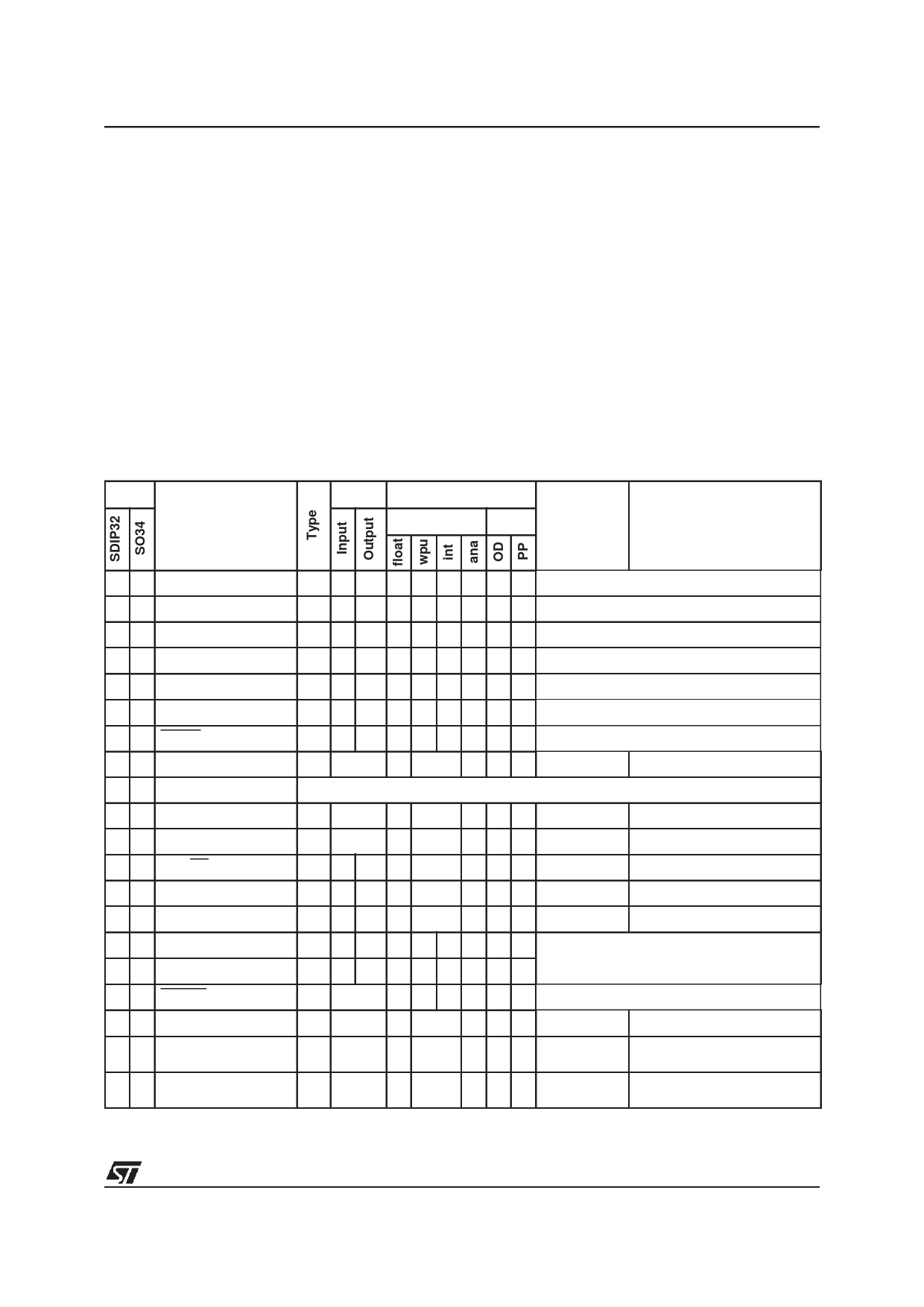
Table 1. Device Pin Description
Pin n°
Pin Name
Level
Port / Control
Input
Main
Output Function
(after reset)
Alternate Function
1 1 MCO5
2 2 MCO4
3 3 MCO3
4 4 MCO2
5 5 MCO1
6 6 MCO0
7 7 MCES
8 8 PB5/MISO
9 NC
9 10 PB4/MOSI
10 11 PB3/SCK
11 12 PB2/SS
12 13 PB1/EXTCLK_B
13 14 PB0/EXTCLK_A
14 15 OSC1
15 16 OSC2
16 17 RESET
17 18 PA0/AIN0
18 19 PA1/ICAP2_B/AIN1
19 20 PA2/ICAP1_B/AIN2
O
C
O
C
O
C
O
C
O
C
O
C
I CT
I/O CT
X
X EI1
I/O CT X EI1
I/O CT X EI1
I/O CT HS X EI1
I/O CT HS X EI1
I/O CT HS X EI1
I/O C
X
I/O CT X EI0
I/O CT X EI0
I/O CT X EI0
X Motor Control Output Channel 5
X Motor Control Output Channel 4
X Motor Control Output Channel 3
X Motor Control Output Channel 2
X Motor Control Output Channel 1
X Motor Control Output Channel 0
Motor Control Emergency Stop Input
X X Port B5
SPI Master In / Slave Out Data
Not Connected
X X Port B4
SPI Master Out / Slave In Data
X X Port B3
SPI Serial Clock
T
Port B2
SPI Slave Select (active low)
T
Port B1
Timer B Input Clock
T
Port B0
Timer A Input Clock
These pins connect a crystal or ceramic
resonator, or an external RC, or an external
source to the on-chip oscillator
X
Top priority non maskable interrupt (active low)
X X X Port A0
X X X Port A1
X X X Port A2
ADC Analog Input 0
Timer B Input Capture 2 or
ADC Analog Input 1
Timer B Input Capture 1 or
ADC Analog Input 2
7/132
6
Share Link: 