MTP805N View Datasheet(PDF) - Unspecified
Part Name
Description
Manufacturer
MTP805N Datasheet PDF : 15 Pages
| |||
MYSON
TECHNOLOGY
MTP805
(Rev. 0.9)
3. I/O Pin Usage
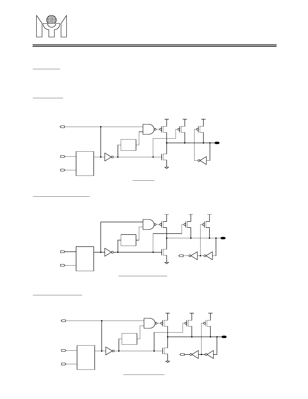
3.1 KSO0~7
These pins are direct output from the 8051’s Port1 and dedicated for key scan output. The pin’s input
function is removed. Read 8051’s Port1 is only read the data in the Port1’s output register. These pins are
“Pseudo open-drain” structure.
3.2 KSO8~15
These pins are direct output from the 8051’s Port2 and dedicated for key scan output. The pin’s input
function is removed. Read 8051’s Port2 is only read the data in the Port2’s output register. These pins are
“Pseudo open-drain” structure.
Read
Data
Write
Data
/WR
D
Q
Output
Register
CK
2 OSC
period
delay
4mA
50uA
500uA
Pin
4mA
KSO0~15
3.3 KSO16~17, GPIO0~1
These pins are output from MTP805’s XFR. They can be used as key scan output or general purpose I/O.
Read these pins will read the data on pin. These pins are also “Pseudo open-drain” structure.
Write
Data
/WR
D
Q
Output
Register
CK
4mA
50uA
1 OSC
period
delay
4mA
Read
Data
KSO16~17, GPIO0~1
500uA
Pin
3.4 MSCLK, MSDATA
These pins are connected to 8051’s P3.1 and P3.0. The usage of these pins are the same as standard 8051
except the UART’s function being not provided. These pins are also “Pseudo open-drain” structure.
Read
Latch
Data
Write
Data
/WR
D
Q
Output
Register
CK
Revision 0.9
4mA
50uA
2 OSC
period
delay
4mA
Read
Pin
Data
MSCLK, MSDATA
500uA
Pin
-5-
2000/07/19
Share Link: 