MTP805N View Datasheet(PDF) - Unspecified
Part Name
Description
Manufacturer
MTP805N Datasheet PDF : 15 Pages
| |||
MYSON
TECHNOLOGY
MTP805
(Rev. 0.9)
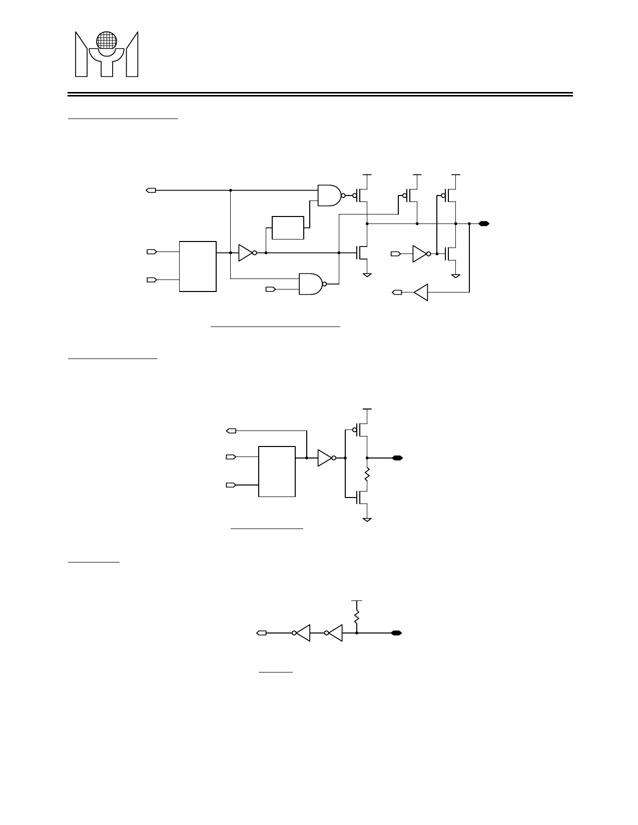
3.5 PS2CLK, PS2DATA
These pins are shared with USB’s DP/DM pins. They are connected to 8051’s P3.4 and P3.5. In PS2 mode,
S/W should keep “ENUSB”=0 and “PS2KB”=1. In USB mode, S/W should keep “ENUSB”=1, “PS2KB”=0 and
P3.4/P3.5 output high. These pins are also “Pseudo open-drain” structure in PS2 mode.
3.3V
Read
Latch
Data
2 OSC
period
delay
4mA
20uA
Pin
Write
Data
/WR
D
Q
Output
Register
CK
PS2KB
DP/PS2CLK, DM/PS2DATA
4mA
USBSIE
Output
Read
Pin
Data
3.6 LED0~2, GPO0
These pins are used to drive LED. Basically, they are open-drain structure. Each one has a 420 ohm serial
resistor when sink pin to low, and has a 100K resistor when drive high. S/W may write data to “LED” register
to control these pins’status. Read “LED” only read the data in the “LED” register, instead of data on the pins.
Read
Data
Write
Data
/WR
D
Q
Output
Register
CK
LED0~2, GPO0
50uA
Pin
420
4mA
3.7 KSI0~7
These pins are used as key scan input. Reading “KSI” register of XFR reflect the data on the pin. These pins
are input only with pull-up resistor on each pin.
Read
Pin
Data
KSI0~7
Revision 0.9
-6-
2000/07/19
Share Link: 