LTC1041MJ8 View Datasheet(PDF) - Linear Technology
Part Name
Description
Manufacturer
LTC1041MJ8 Datasheet PDF : 8 Pages
| |||
LTC1041
ABSOLUTE AXI U RATI GS
(Note 1)
Total Supply Voltage (V+ to V –) .............................. 18V
Input Voltage ........................ (V+ + 0.3V) to (V – – 0.3V)
Operating Temperature Range
LTC1041C ......................................... –40°C to 85°C
LTC1041M (OBSOLETE) .................. – 55°C to125°C
Storage Temperature Range ................. – 55°C to 150°C
Lead Temperature (Soldering, 10 sec).................. 300°C
Output Short Circuit Duration ....................... Continuous
UW U
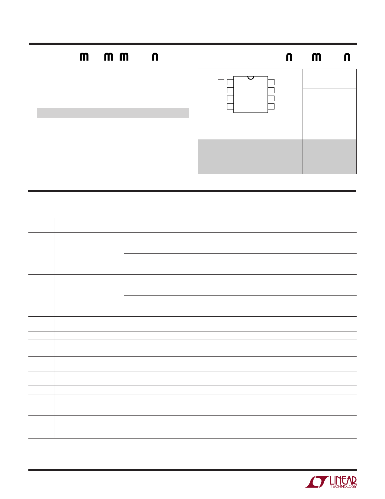
PACKAGE/ORDER I FOR ATIO
ON / OFF 1
VIN 2
SET POINT 3
GND 4
TOP VIEW
8 V+
7 VP-P
6 OSC
5 DELTA
ORDER PART
NUMBER
LTC1041CN8
LTC1041CS8
N8 PACKAGE
8-LEAD PDIP
S8 PACKAGE
8-LEAD PDIP
TJMAX = 110°C, θJA = 150°C/W (N8)
TJMAX = 150°C, θJA = 150°C/W (S8)
J8 PACKAGE
8-LEAD CERDIP
TJMAX = 150°C, θJA = 100°C/W
OBSOLETE PACKAGE
Consider the N8 Package as an Alternate Source
LTC1041MJ8
Consult LTC Marketing for parts specified with wider operating temperature ranges.
ELECTRICAL CHARACTERISTICS The q denotes the specifications which apply over the full operating
temperature range, otherwise specifications are at TA = 25°C. Test Conditions: V+ = 5V, unless otherwise specified.
SYMBOL PARAMETER
CONDITIONS
TC1041M/LTC1041C
MIN
TYP
MAX
UNITS
SET POINT Error (Note 3)
V+ = 2.8V to 6V (Note 2)
V+ = 6V to 15V (Note 2)
Deadband Error (Note 4)
V+ = 2.8V to 6V (Note 2)
V+ = 6V to 15V (Note 2)
IOS
Input Current
V + = 5V, TA = 25°C, OSC = GND
(VIN, SET POINT and DELTA Inputs)
RIN
Equivalent Input Resistance fS = 1kHz (Note 5)
Input Voltage Range
q
q
q
q
q 10
q GND
±0.3
+
± 0.05
±1
+
± 0.05
±0.6
+
±0.1
±2
+
±0.1
±0.3
15
±0.5
mV
+
±0.1 % of DELTA
±3
mV
+
±0.1 % of DELTA
±1
mV
+
±0.2 % of DELTA
±6
+
±0.2 % of DELTA
nA
MΩ
V+
V
PSR
IS(ON)
Power Supply Range
Power Supply ON
Current (Note 6)
V + = 5V, VP-P ON
q 2.8
16
V
q
1.2
3
mA
IS(OFF)
Power Supply OFF
V + = 5V, VP-P OFF LTC1041C
q
Current (Note 6)
LTC1041M
q
0.001
0.5
µA
0.001
5
µA
tD
Response Time (Note 7)
V + = 5V
60
80
100
µs
ON/OFF Output (Note 8)
VOH
VOL
Logical “1” Output Voltage
Logical “0” Output Voltage
V
V
+
+
=
=
4.75V,
4.75V,
IOUT
IOUT
=
=
–360µA
1.6mA
q 2.4
4.4
V
0.25
0.4
V
REXT
External Timing Resistor
Resistor Connected between V+ and OSC Pin
q 100
10,000
kΩ
fS
Sampling Frequency
V + = 5V, TA = 25°C,
REXT = 1M CEXT = 0.1µF
5
Hz
Note 1: Absolute Maximum Ratings are those values beyond which the life
of a device may be impaired.
Note 2: Applies over input voltage range limit and includes gain
uncertainty.
1041fa
2
Share Link: 