NTE7131 View Datasheet(PDF) - NTE Electronics
Part Name
Description
Manufacturer
NTE7131 Datasheet PDF : 4 Pages
| |||
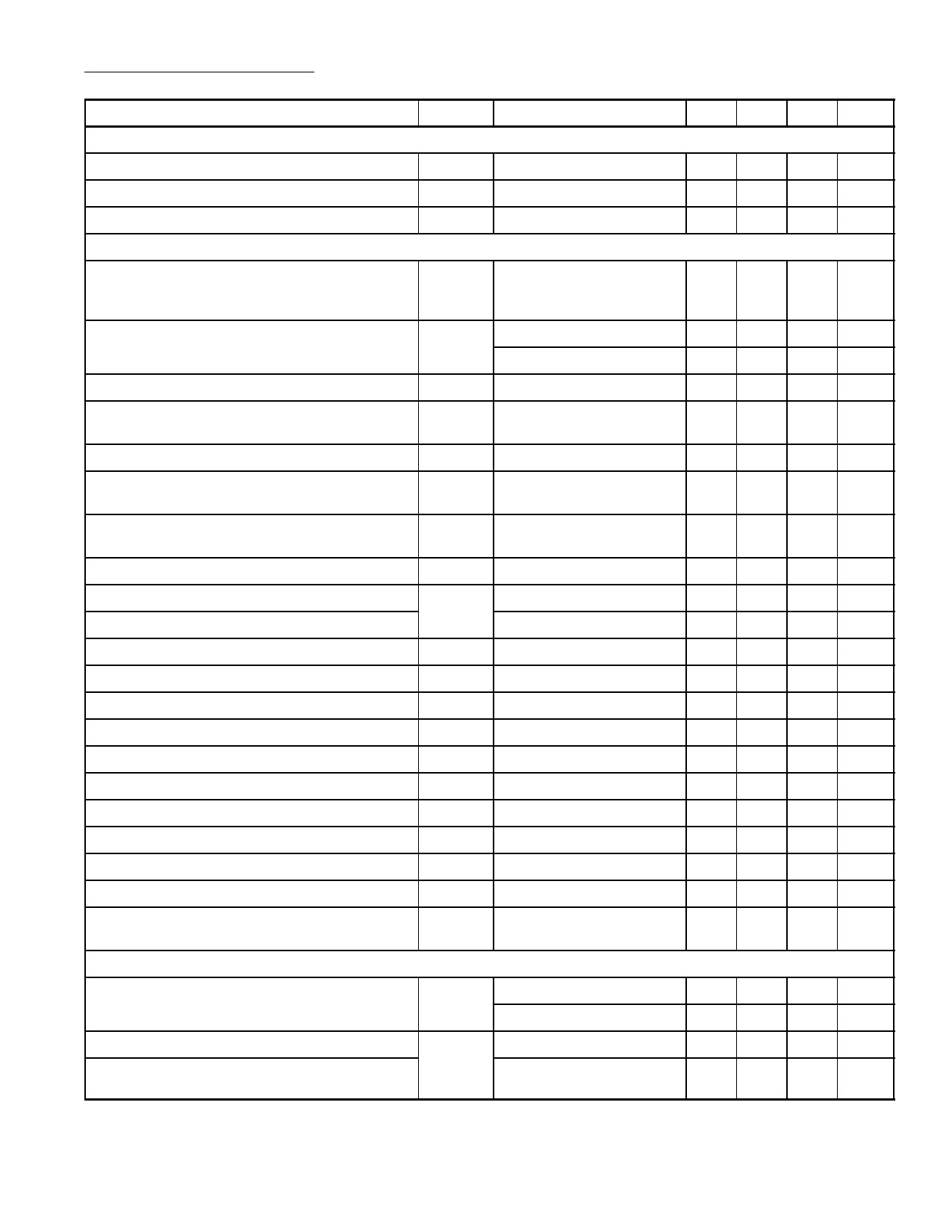
Electrical Characteristics: (VP = 14.5V, TA = +25°C, VFB = 45V, fi = 50Hz, II(sb) = 400µA unless
otherwise specified)
Parameter
Symbol
Test Conditions
Min Typ Max Unit
DC Supply
Operating Supply Voltage
Flyback Supply Voltage
Supply Current
Vertical Circuit
VP
VFB
IP No Signal, No Load
9.0 4.5 25.0 V
VP
–
50
V
– 30 55 mA
Output Voltage Swing (Scan)
Linearity Error
Output Voltage Swing (Flyback) VO(A) – VO(B)
Forward Voltage of the Internal Efficiency
Diode (VO(A) – VFB)
Output Offset Current
Offset Voltage at the Input of the Feedback
Amplifier (VI(fb) – VO(B))
Output Offset Voltage as a Function of
Temperature
VO
Idiff = 0.6mA(p–p),
Vdiff = 1.8V(p–p),
IO = 2A(p–p)
13.2 –
LE IO = 2A(p–p), Note 3
–
1
IO = 50mA(p–p), Note 3
–
1
VO Idiff = 0.3mA, IO = 1A (M)
–
40
VDF IO = –1A (M), Idiff = 0.3mA –
–
|IOS| Idiff = 0, II(sb) = 50 to 500µA –
–
|VOS| Idiff = 0, II(sb) = 50 to 500µA –
–
∆VOST Idiff = 0
–
–
–
V
4
%
4
%
–
V
1.5 V
40 mA
24 mV
72 µV/K
DC Output Voltage
Open–Loop Voltage Gain (V7–4/V1–2)
Open–Loop Voltage Gain (V7–4/V9–4, V1–2 = 0)
Voltage Ratio V1–2/V9–4
Frequency Response (–3dB)
Current Gain (IO/Idiff)
Current Gain Drift as a Function of Temperature
Signal Bias Current
Flyback Supply Current
Power Supply Ripple Rejection
VO(A)
Gvo
VR
fres
GI
∆GcT
II(sb)
IFB
PSRR
Idiff = 0, Note 4
Note 5, Note 6
Note 5
Open Loop, Note 7
During Scan
Note 8
– 6.5 –
V
– 80 – dB
– 80 – dB
–
0
–
dB
– 40 – Hz
– 5000 –
–
– 10–4 K
50 400 500 µA
–
– 100 µA
– 80 – dB
DC Input Voltage
Common Mode Input Voltage
Input Bias Current
Common Mode Output Current
Guard Circuit
VI(DC)
VI(CM)
Ibias
IO(CM)
II(sb) = 0
II(sb) = 0
∆II(sb) = 300µA(p–p),
fi = 50Hz, Idiff = 0
– 2.7 –
V
0
– 1.6 V
– 0.1 0.5 µA
– 0.2 – mA
Output Current
Output Voltage on Pin8
Allowable Voltage on Pin8
IO
Not Active, VO(guard) = 0V –
– 50 µA
Active, VO(guard) = 4.5V
1.0 – 2.5 mA
VO(guard) IO = 100µA
–
– 5.5 V
Maximum Leakage
Current = 10µA
–
– 40
V
Share Link: 