MPC2605ZP66R View Datasheet(PDF) - Motorola => Freescale
Part Name
Description
Manufacturer
MPC2605ZP66R Datasheet PDF : 30 Pages
| |||
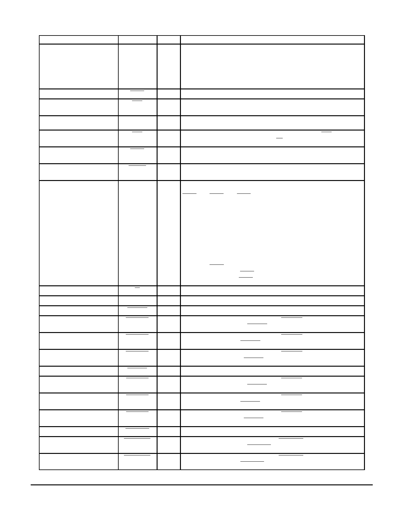
PIN DESCRIPTIONS
Pin Locations
19G, 17H – 19H, 17J – 19J,
17K – 19K, 17L – 19L,
17M – 19M, 17N – 19N,
17P – 19P, 17R – 19R,
18T, 19T, 18U, 19U,
18V, 19V, 18W *
Pin Name
A0 – A31
Type
I/O
Description
Address inputs from processor. Can also be outputs for processor snoop
addresses. A0 is the MSB. A31 is the LSB.
3G
AACK
I/O Address acknowledge input/output.
2A
ABB
I/O Used as an input to qualify bus grants. Driven as an output during address tenure
initiated by the MPC2605.
* 17C – 19C, 17D
AP0 – AP3
I/O Address parity.
19B
APE
O Address parity error. When an address parity error is detected, APE will be driven
low one clock cycle after the assertion of TS then High–Z following clock cycle.
18E
APEN
I
Address parity enable. When tied low, enables address parity bits and the
address parity error bit.
1G
ARTRY
I/O Address retry status I/O. Generated when a read or write snoop to a dirty
processor cache line has occurred.
2U
CFG0
I
Configuration inputs. These must be tied to either VDD or VSS.
2V
CFG1
CFG0
CFG1
CFG2
1V
CFG2
0
0
0
256KB
17E
CFG3
0
1
0
512KB; A26 = 0
2B
CFG4
0
1
1
512KB; A26 = 1
1
0
0
1MB; A25 – A26 = 00
1
0
1
1MB; A25 – A26 = 01
1
1
0
1MB; A25 – A26 = 10
1
1
1
1MB; A25 – A26 = 11
CFG3
Snoop Data Tenure Selector
0 Supports snoop data tenure
1 Does not support snoop data tenure
CFG4
AACK Driver Enable
0 Disable AACK driver
1 Enable AACK driver
2G
CI
I/O Cache inhibit I/O.
3M
CLK
I
Clock input. This must be the same as the processor clock input.
2M
CPU BG
I
CPU bus grant input.
3E
CPU2 BG
I
MPC2605 logically ORs this signal with CPU BG. Used in multiprocessor
configuration as the second CPU BG.
1B
CPU3 BG
I
MPC2605 logically ORs this signal with CPU BG. Used in multiprocessor
configuration as the third CPU BG.
1T
CPU4 BG
I
MPC2605 logically ORs this signal with CPU BG. Used in multiprocessor
configuration as the fourth CPU BG.
2H
CPU BR
I
CPU bus request input.
2D
CPU2 BR
I
MPC2605 logically ORs this signal with CPU BR. Used in multiprocessor
configuration as the second CPU BR.
2C
CPU3 BR
I
MPC2605 logically ORs this signal with CPU BR. Used in multiprocessor
configuration as the third CPU BR.
1U
CPU4 BR
I
MPC2605 logically ORs this signal with CPU BR. Used in multiprocessor
configuration as the fourth CPU BR.
1F
CPU DBG
I
CPU data bus grant input from arbiter.
3D
CPU2 DBG
I
MPC2605 logically ORs this signal with CPU DBG. Used in multiprocessor
configuration as the second CPU DBG.
3C
CPU3 DBG
I
MPC2605 logically ORs this signal with CPU DBG. Used in multiprocessor
configuration as the third CPU DBG.
* See pin diagram (page 2) for specific pin assignment of these bus signals.
MOTOROLA
MPC2605
3
Share Link: 