MPC2605ZP66R View Datasheet(PDF) - Motorola => Freescale
Part Name
Description
Manufacturer
MPC2605ZP66R Datasheet PDF : 30 Pages
| |||
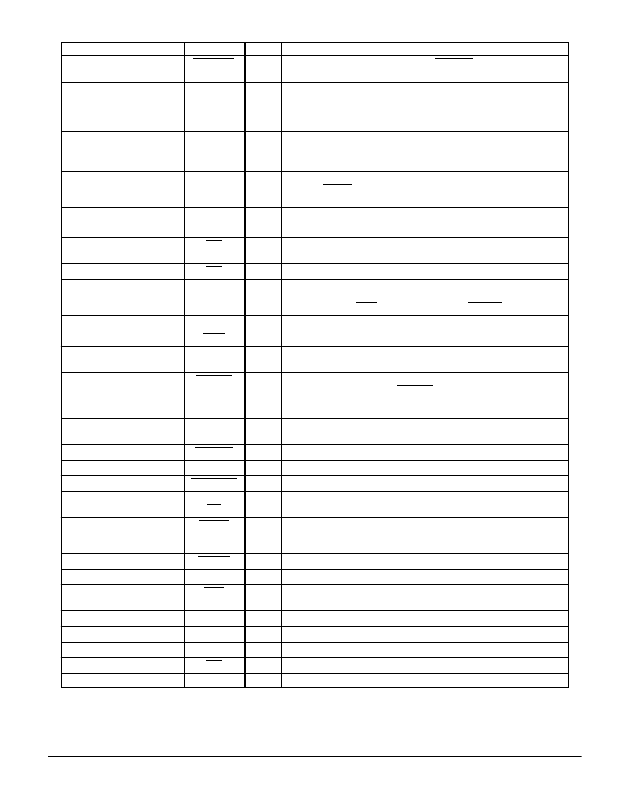
Pin Locations
2T
Pin Name
CPU4 DBG
Type
I
Description
MPC2605 logically ORs this signal with CPU DBG. Used in multiprocessor
configuration as the fourth CPU DBG.
11A – 13A, 15A – 18A,
11B – 17B, 11C, 12C, 10U,
11U, 10V – 12V, 14V – 17V,
11W – 17W *
DL0 – DL31
I/O Data bus low input and output. DL0 is the MSB. DL31 is the LSB.
4A – 10A, 4B – 10B, 6C,
10C, 8U, 9U, 3V – 6V,
8V, 9V, 3W –10W *
DH0 – DH31 I/O Data bus high input and output. DH0 is the MSB. DH31 is the LSB.
2J
DBB
I/O Data bus busy. Used as input when processor is master, driven as an output after
a qualified L2 DBG when MPC2605 is the bus master. Note: To operate in Fast
L2 mode, this pin must be tied high.
14A, 18B, 5C, 8C,
16U, 7V, 13V, 2W *
DP0 – DP7
I/O Data bus parity input and output.
1C
FDN
I/O Flush done I/O used for communication between other MPC2605 devices. Must
be tied together between all MPC2605 parts along with a pullup resistor.
19E
GBL
O Global transaction. Always negated when MPC2604 is bus master.
1J
HRESET
I
Hard reset input from processor bus. This is an asynchronous input that must be
low for at least 16 clock cycles to ensure the MPC2605 is properly reset. For
proper initialization, TRST must be asserted before HRESET is asserted.
3A
L2 BG
I
Bus grant input from arbiter.
1D
L2 BR
I/O Bus request I/O. Normally used as an output.
19D
L2 CI
I
Secondary cache inhibit sampled, after assertion of TS. Assertion prevents
linefill.
2F
L2 CLAIM
O L2 cache claim output. Used to claim the bus for processor initiated memory
operations that hit the L2 cache. L2 CLAIM goes true (low) before the rising edge
of CLK following TS true. Because this output is not always driven, a pullup
resistor may be necessary to ensure proper system functioning.
2E
L2 DBG
I
Data bus grant input. Comes from system arbiter, used to start data tenure for
bus operations where MPC2605 is the bus master.
18D
L2 FLUSH
I
Causes cache to write back dirty lines and clears all tag valid bits.
3B
L2 MISS INH
I
Prevents line fills on misses when asserted.
2N
L2 TAG CLR
I
Invalidates all tags and holds cache in a reset condition.
3N
L2 UPDATE
I
Cache disable. When asserted, the MPC2605 will not respond to signals on the
INH
local bus and internal states do not change.
3J
PWRDN
I
Provides low power mode. Prevents address and data transitions into the RAM
array. MPC2605 becomes active 4 µs after deassertion. Clock must be externally
disabled.
1N
SRESET
I
Soft reset input from processor bus.
1E
TA
I/O Transfer acknowledge status I/O from processor bus.
3K
TBST
I/O Transfer burst status I/O from processor bus. Used to distinguish between
burstable and non–burstable memory operations.
2P
TCK
I
Test clock input for IEEE 1149.1 boundary scan (JTAG).
1P
TDI
I
Test data input for IEEE 1149.1 boundary scan (JTAG).
1R
TDO
O Test data output for IEEE 1149.1 boundary scan (JTAG).
1H
TEA
I
Transfer error acknowledge status input from processor bus.
3P
TMS
I
Test mode select for IEEE 1149.1 boundary scan (JTAG).
* See pin diagram (page 2) for specific pin assignment of these bus signals.
MPC2605
4
MOTOROLA
Share Link: 