TCM810J View Datasheet(PDF) - Microchip Technology
Part Name
Description
Manufacturer
TCM810J Datasheet PDF : 14 Pages
| |||
TCM809/TCM810
1.0 ELECTRICAL
CHARACTERISTICS
Absolute Maximum Ratings†
Supply Voltage (VDD to GND) ..........................................6.0V
RESET, RESET.................................... – 0.3V to (VDD +0.3V)
Input Current, VDD.........................................................20 mA
Output Current, RESET, RESET...................................20 mA
dV/dt (VDD) ............................................................. 100V/µsec
Operating Temperature Range.................... – 40°C to +125°C
Power Dissipation (TA = 70°C):
3-Pin SOT-23B (derate 4 mW/°C above +70°C) ......320 mW
3-Pin SC-70 (derate 2.17 mW/°C above +70°C)......174 mW
Storage Temperature Range ....................... – 65°C to +150°C
Maximum Junction Temperature, TJ.............................. 150°C
† Notice: Stresses above those listed under “Maximum ratings” may
cause permanent damage to the device. This is a stress rating only and
functional operation of the device at those or any other conditions
above those indicated in the operational listings of this specification is
not implied. Exposure to maximum rating conditions for extended peri-
ods may affect device reliability.
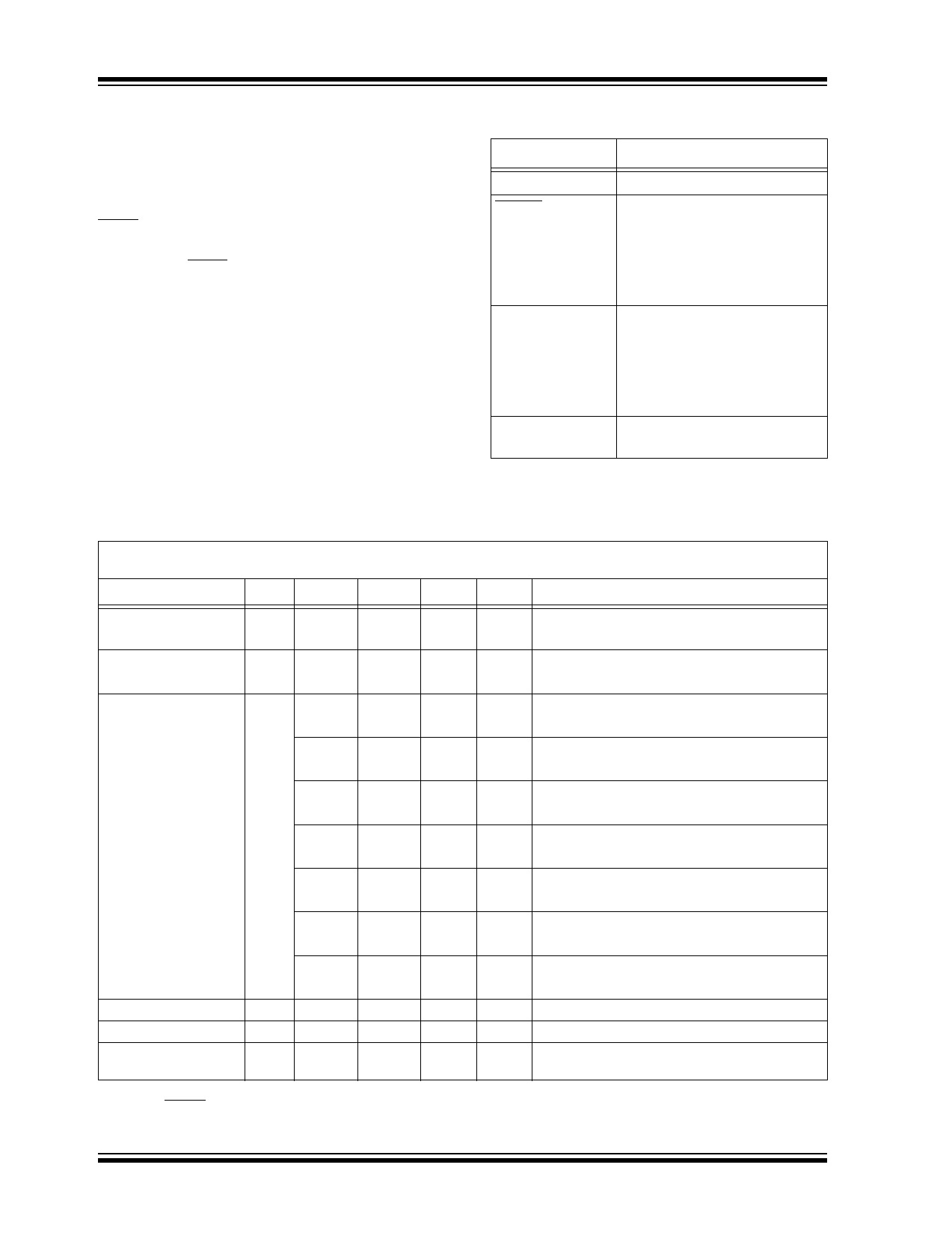
PIN FUNCTION TABLE
NAME
FUNCTION
GND
Ground.
RESET (TCM809)
RESET push-pull output
remains low while VDD is below
the reset voltage threshold and
for 240 msec (140 msec min.)
after VDD rises above reset
threshold.
RESET (TCM810)
RESET push-pull output
remains high while VDD is below
the reset voltage threshold and
for 240 msec (140 msec min.)
after VDD rises above reset
threshold.
VDD
Supply voltage (+2.5V, +3.0V,
+3.3V, +5.0V).
ELECTRICAL CHARACTERISTICS
VDD = Full Range, TA = Operating Temperature Range, unless otherwise noted. Typical values are at TA = +25°C,
VDD = 5V for L/M/J, 3.3V for T/S, 3.0V for R and 2.5V for Z (Note 1).
Parameter
Sym
Min
Typ
Max Units
Test Conditions
VDD Range
Supply Current
ICC
Reset Threshold (Note 2) VTH
Reset Threshold Tempco
1.0
1.2
—
—
4.56
4.50
4.31
4.25
3.93
3.89
3.04
3.00
2.89
2.85
2.59
2.55
2.28
2.25
—
—
5.5
V TA = 0°C to +70°C
—
5.5
TA = – 40°C to +125°C
12
30
µA TCM8xxL/M/J: VDD < 5.5V
9
25
TCM8xxR/S/T/Z: VDD < 3.6V
4.63
4.70
V TCM8xxL:
TA = +25°C
—
4.75
TA = – 40°C to +125°C
4.38
4.45
V TCM8xxM:
TA = +25°C
—
4.50
V
TA = – 40°C to +125°C
4.00
4.06
V TCM809J:
TA = +25°C
—
4.10
V
TA = – 40°C to +125°C
3.08
3.11
V TCM8xxT:
TA = +25°C
—
3.15
V
TA = – 40°C to +125°C
2.93
2.96
V TCM8xxS:
TA = +25°C
—
3.00
V
TA = – 40°C to +125°C
2.63
2.66
V TCM8xxR:
TA = +25°C
—
2.70
V
TA = – 40°C to +125°C
2.32
2.35
V TCM8xxZ:
TA = +25°C
—
2.38
V
TA = – 40°C to +125°C
30
— ppm/°C
VDD to Reset Delay,
Reset Active Time Out
Period
—
65
—
µsec VDD = VTH to (VTH – 100 mV) (Note 2)
140
320
560 msec
Note 1: Production testing done at TA = +25°C, overtemperature limits ensured by QC screen.
2: RESET output for TCM809, RESET output for TCM810.
DS21661C-page 2
2004 Microchip Technology Inc.
Share Link: 