AT42QT1110-MU(2010) View Datasheet(PDF) - Atmel Corporation
Part Name
Description
Manufacturer
AT42QT1110-MU Datasheet PDF : 48 Pages
| |||
AT42QT1110-MU/AT42QT1110-AU
3.5 Power Supply
3.5.1
General Considerations
See Section 8.2 on page 38 for the power supply range. If the power supply fluctuates slowly
with temperature, the device tracks and compensates for these changes automatically with only
minor changes in sensitivity. If the supply voltage drifts or shifts quickly, the drift compensation
mechanism is not able to keep up, causing sensitivity anomalies or false detections.
The usual power supply considerations with QT parts apply to the device. The power should be
clean and come from a separate regulator if possible. However, this device is designed to
minimize the effects of unstable power, and, except in extreme conditions, should not require a
separate Low Dropout (LDO) regulator.
See underneath Figure 1.3 on page 4 for suggested regulator manufacturers.
Caution: A regulator IC shared with other logic can result in erratic operation and is
not advised.
A single ceramic 0.1 µF bypass capacitor, with short traces, should be placed very
close to the power pins of the IC. Failure to do so can result in device oscillation,
high current consumption, erratic operation etc.
It is assumed that a larger bypass capacitor (like1 µF) is somewhere else in the power circuit; for
example, near the regulator.
3.5.2
Brownout Detection
The QT1110 includes a power supply monitoring circuit that detects if Vdd drops below a safe
operating voltage. When this occurs, the device goes into a “Reset” state, where no acquisition
or processing is carried out. The device remains in this state until Vdd returns to the specified
voltage range.
Once a safe operating voltage is detected, the QT1110 behaves as per normal power-on/reset
conditions; that is, any saved settings are restored from EEPROM, the internal self-tests are run
and all channels are calibrated.
The Brown-out detector threshold is 2.7V ±10 percent.
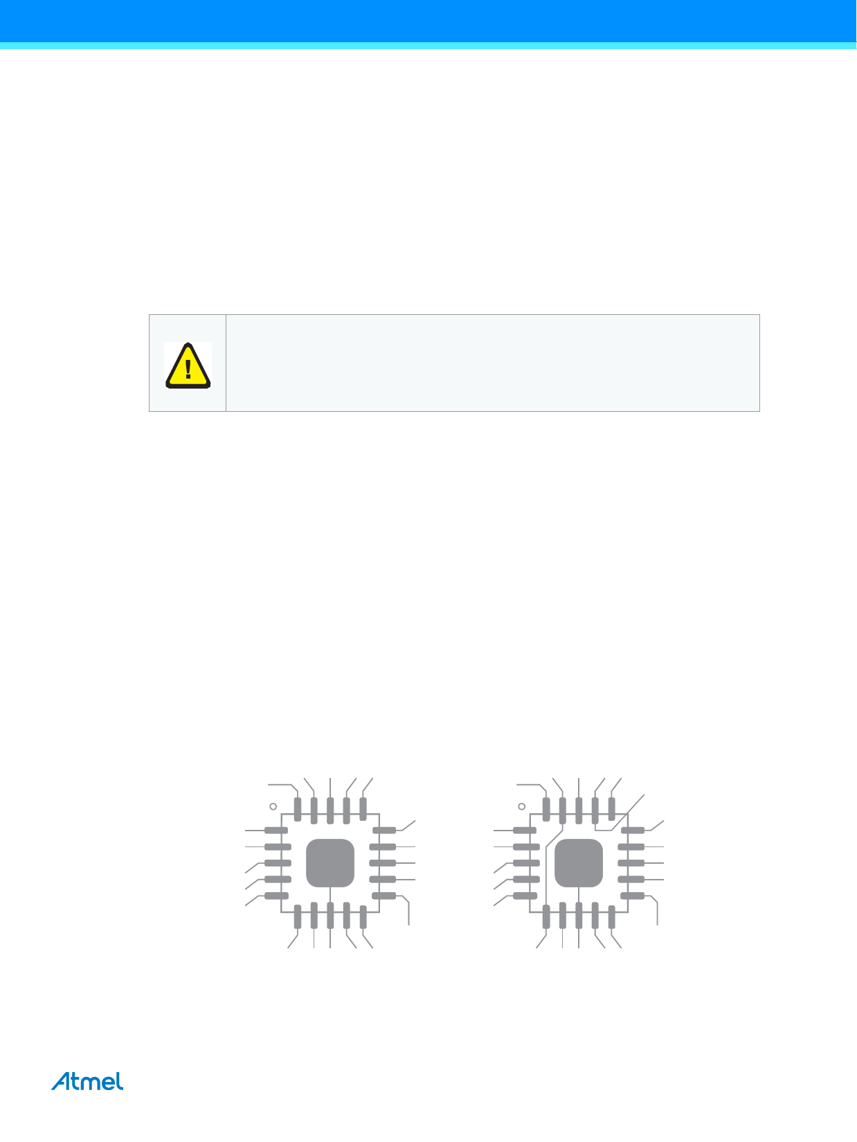
3.6 MLF Package Restrictions
The central pad on the underside of the MLF chip should be connected to ground. Do not run
any tracks underneath the body of the chip, only ground. Figure 3-1 shows an example of
good/bad tracking.
Figure 3-1. Examples of Good and Bad Tracking
Example of GOOD Tracking
Example of BAD Tracking
9
9520I–AT42–03/10
Share Link: 