MT6162N View Datasheet(PDF) - MediaTek Inc
Part Name
Description
Manufacturer
MT6162N Datasheet PDF : 32 Pages
| |||
Preliminary Datasheet
MT6162
OPERATING CONDITIONS
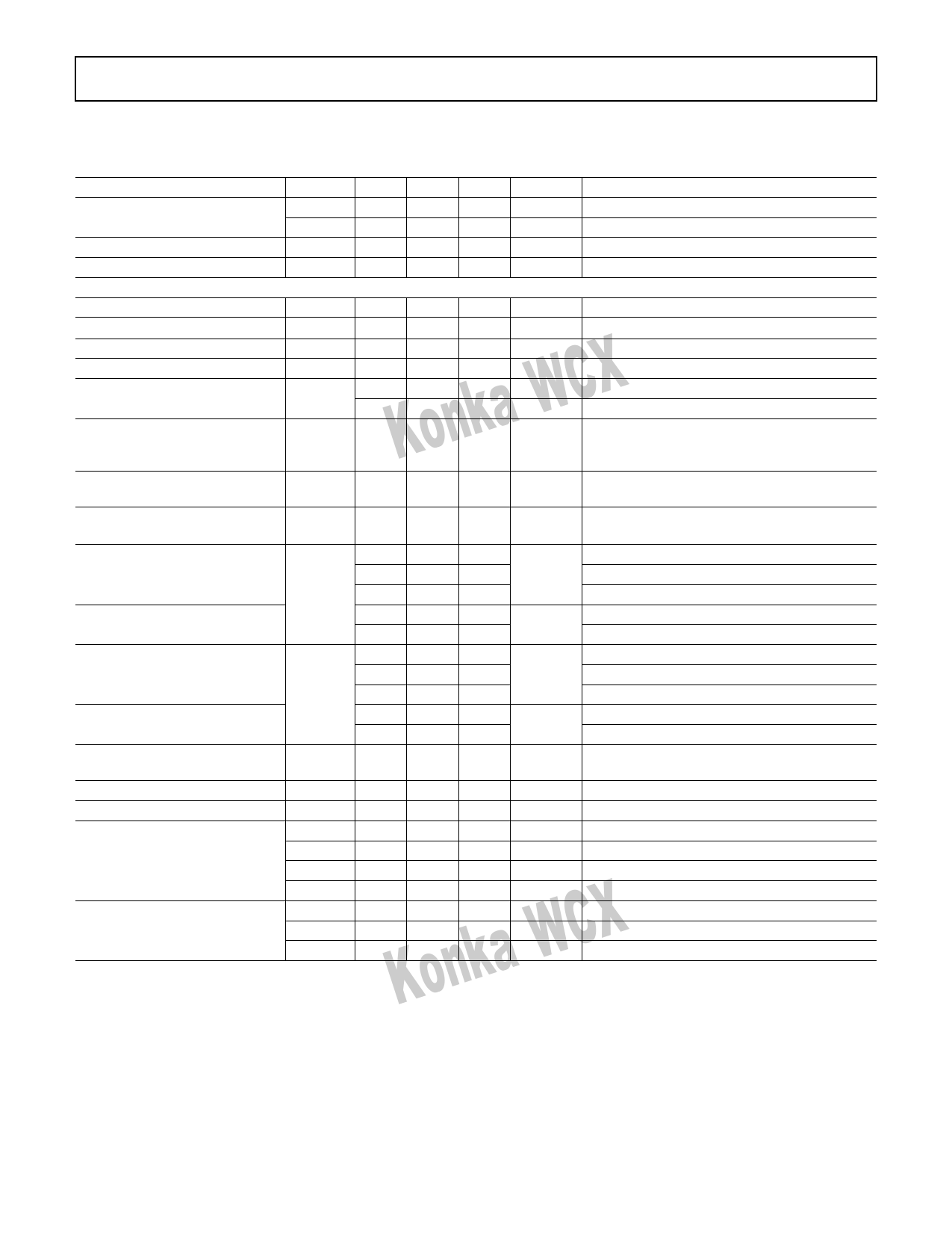
Table 1
Parameter
Symbol Min Typ Max Unit Comments
Reference Supply
VCXO/DCXO Supply
Ambient Temperature
Rx baseband load capacitance
Rx baseband load resistance
Rx required amplitude balance
Rx required phase balance
Tx baseband I/Q common
mode
Tx baseband I/Q differential
Full-Scale input
VDD_28
VDD_18
VINT
VDDXO
Tamb
CLD
RLd
DAdiff
Dfdiff
VCM
2.75 2.85 2.95
V
Linear regulated supply
1.75 1.825 1.9
V
Switching regulated supply
1.675 1.8 1.925
V
Serial interface control logic
2.7 2.8 2.9
V
Linear regulated supply
-30
25
85
10
ºC
pF
Equivalent Differential1)
20
32
45
kΩ
Differential
Konka_WCX -1
1
dB All Rx input pairs
-10
10
deg All Rx input pairs
1.05 1.1 1.15
1.05
1.25
V
V
Acceptable range with slight degradation2)
940 990 1040 mVppd 2.4dB allocated for Tx RF impairments
compensation; 750mVppd effectively used
for I/Q Tx BB signal
Tx baseband I/Q Input
Resistance
200
kΩ Differential
Tx baseband I/Q Input
Capacitance
2.5
pF
Differential
4.0
pF
Single-Ended
High Band (HB) Transmitter
Frequency
1920
1850
1980
1910
MHz
3G Band I
3G Band II / GSM1900
Low Band (LB) Transmitter
Frequency
FTx
1710
824
880
1785
849
915
MHz
3G Band III/IV/IX/X / GSM1800
3G Band V/VI / GSM850
3G Band VIII / GSM900
High Band (HB) Receiver
Frequency
2110
1930
2170
1990
MHz
3G Band I/IV/X
3G Band II / GSM1900
Low Band (LB) Receiver
Frequency
FRx
1805
869
925
1880
894
960
MHz
3G Band III/IX / GSM1800
3G Band V/VI / GSM850
3G Band VIII / GSM900
Reference Input Clock
(VCTCXO) Frequency
Voltage Swing
Duty Cycle
Fref
26
MHz
700
1500 mVpp
40
60
%
Reference Input Clock
(VCTCXO) Phase Noise
-106
-134
dBc/Hz
dBc/Hz
@ Foffset = 100Hz
@ Foffset = 1KHz
-144 dBc/Hz @ Foffset = 10KHz
Konka_WCX Harmonic Content
-148
-8
dBc/Hz @ Foffset = 100KHz
dBc HD2 @ 52MHz
-10
dBc HD3 @ 78MHz
-20
dBc HD4 @ 104MHz
1) VCM up to 1.25V causes no performance degradation for nominal silicon over ETC. For worst-case silicon, a ~1dB degradation in full chain
ACLR can be expected.
2) The load capacitance can be either common mode (to AC ground) or differential. The specification is written in terms of an equivalent
differential load capacitance. In reality, the split can be arbitrary between common mode and differential mode, and both scenarios must be
considered. The maximum difference between CRX-GND and CRXB-GND is 1pF.
REV. (1.3) FEB 7th 2011
- 6 - MediaTek Proprietary & Confidential Information
Share Link: 