AD632TD View Datasheet(PDF) - Analog Devices
Part Name
Description
Manufacturer
AD632TD Datasheet PDF : 12 Pages
| |||
AD632
Data Sheet
PIN CONFIGURATIONS AND FUNCTION DESCRIPTIONS
VOS
Y2
Z2 (GND)
9
8
10
X2
Y1 1
7
AD632
6 X1
2
+VS
3
Z1
(Not to Scale)
5
4
–VS
OUT
Z1 1
OUT 2
14 +VS
13 Y1
–VS 3 AD632 12 Y2
NC 4 TOP VIEW 11 VOS
NC 5 (Not to Scale) 10 Z2
NC 6
9 X2
X1 7
8 NC
NC = NO CONNECT
Figure 2. Pin Configuration, H-Package, TO-100
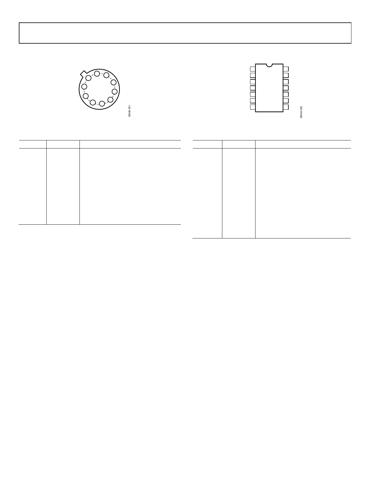
Figure 3. Pin Configuration, D-Package, SBDIP
Table 3. Pin Function Descriptions, 10-Pin TO-100
Pin No. Mnemonic Description
1
Y1
Y Multiplicand Noninverting Input.
2
+VS
Positive Supply Voltage.
3
Z1
Summing Node Noninverting Input.
4
OUT
Product.
5
−VS
Negative Supply Voltage.
6
X1
X Multiplicand Noninverting Input.
7
X2
X Multiplicand Inverting Input.
8
Z2
Summing Node Inverting Input.
9
VOS
Offset Voltage Adjustment.
10
Y2
Y Multiplicand Inverting Input.
Table 4. Pin Function Descriptions, 14-Lead SBDIP
Pin No. Mnemonic Description
1
Z1
Summing Node Noninverting Input.
2
OUT
Product.
3
−VS
Negative Supply Voltage.
4, 5, 6, 8 NC
No Connection. Do not connect to
this pin.
7
X1
X Multiplicand Noninverting Input.
9
X2
X Multiplicand Noninverting Input.
10
Z2
Summing Node Inverting Input.
11
VOS
Offset Voltage Adjustment.
12
Y2
Y Multiplicand Inverting Input.
13
Y1
Y Multiplicand Noninverting Input.
14
+VS
Positive Supply Voltage.
Rev. D | Page 6 of 12
Share Link: 