SST25VF016B View Datasheet(PDF) - Microchip Technology
Part Name
Description
Manufacturer
SST25VF016B Datasheet PDF : 30 Pages
| |||
SST25VF016B
3.0 MEMORY ORGANIZATION
The SST25VF016B SuperFlash memory array is orga-
nized in uniform 4 KByte erasable sectors with
32 KByte overlay blocks and 64 KByte overlay eras-
able blocks.
4.0 DEVICE OPERATION
The SST25VF016B is accessed through the SPI (Serial
Peripheral Interface) bus compatible protocol. The SPI
bus consist of four control lines; Chip Enable (CE#) is
used to select the device, and data is accessed through
the Serial Data Input (SI), Serial Data Output (SO), and
Serial Clock (SCK).
The SST25VF016B supports both Mode 0 (0,0) and
Mode 3 (1,1) of SPI bus operations. The difference
between the two modes, as shown in Figure 4-1, is the
state of the SCK signal when the bus master is in
Stand-by mode and no data is being transferred. The
SCK signal is low for Mode 0 and SCK signal is high for
Mode 3. For both modes, the Serial Data In (SI) is sam-
pled at the rising edge of the SCK clock signal and the
Serial Data Output (SO) is driven after the falling edge
of the SCK clock signal.
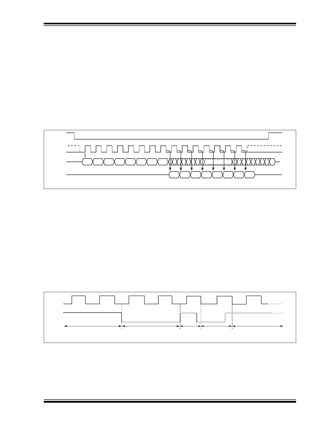
FIGURE 4-1:
SPI PROTOCOL
CE#
MODE 3
SCK MODE 0
MODE 3
MODE 0
SI
Bit 7 Bit 6 Bit 5 Bit 4 Bit 3 Bit 2 Bit 1 Bit 0
DON'T CARE
MSB
HIGH IMPEDANCE
SO
Bit 7 Bit 6 Bit 5 Bit 4 Bit 3 Bit 2 Bit 1 Bit 0
MSB
1271 SPIprot.0
4.1 Hold Operation
The HOLD# pin is used to pause a serial sequence
underway with the SPI flash memory without resetting
the clocking sequence. To activate the HOLD# mode,
CE# must be in active low state. The HOLD# mode
begins when the SCK active low state coincides with
the falling edge of the HOLD# signal. The HOLD mode
ends when the HOLD# signal’s rising edge coincides
with the SCK active low state.
If the falling edge of the HOLD# signal does not coin-
cide with the SCK active low state, then the device
enters Hold mode when the SCK next reaches the
active low state. Similarly, if the rising edge of the
HOLD# signal does not coincide with the SCK active
low state, then the device exits in Hold mode when the
SCK next reaches the active low state. See Figure 4-2
for Hold Condition waveform.
Once the device enters Hold mode, SO will be in high-
impedance state while SI and SCK can be VIL or VIH.
If CE# is driven active high during a Hold condition, it
resets the internal logic of the device. As long as
HOLD# signal is low, the memory remains in the Hold
condition. To resume communication with the device,
HOLD# must be driven active high, and CE# must be
driven active low. See Figure 5-3 for Hold timing.
FIGURE 4-2:
HOLD CONDITION WAVEFORM
SCK
HOLD#
Active
Hold
4.2 Write Protection
SST25VF016B provides software Write protection. The
Write Protect pin (WP#) enables or disables the lock-
down function of the status register. The Block-Protec-
tion bits (BP3, BP2, BP1, BP0, and BPL) in the status
Active
Hold
Active
1271 HoldCond.0
register provide Write protection to the memory array
and the status register. See Table 4-3 for the Block-Pro-
tection description.
2015 Microchip Technology Inc.
Downloaded from: http://www.datasheetcatalog.com/
DS20005044C-page 5
Share Link: 