SST25VF016B View Datasheet(PDF) - Microchip Technology
Part Name
Description
Manufacturer
SST25VF016B Datasheet PDF : 30 Pages
| |||
SST25VF016B
4.2.1 WRITE PROTECT PIN (WP#)
The Write Protect (WP#) pin enables the lock-down
function of the BPL bit (bit 7) in the status register.
When WP# is driven low, the execution of the Write-
Status-Register (WRSR) instruction is determined by
the value of the BPL bit (see Table 4-1). When WP# is
high, the lock-down function of the BPL bit is disabled.
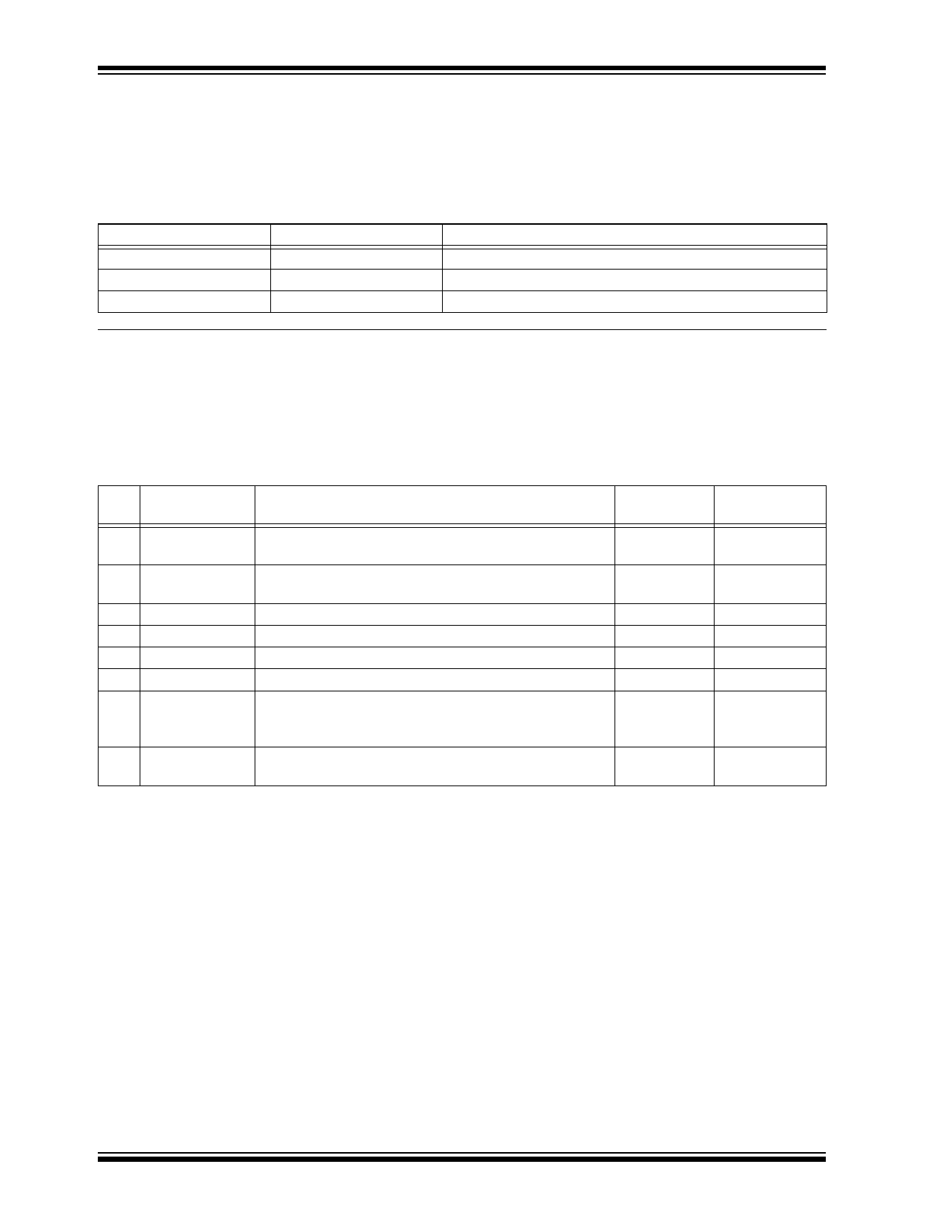
TABLE 4-1: CONDITIONS TO EXECUTE WRITE-STATUS-REGISTER (WRSR) INSTRUCTION
WP#
BPL
Execute WRSR Instruction
L
1
Not Allowed
L
0
Allowed
H
X
Allowed
4.3 Status Register
The software status register provides status on
whether the flash memory array is available for any
Read or Write operation, whether the device is Write
enabled, and the state of the Memory Write protection.
During an internal Erase or Program operation, the sta-
tus register may be read only to determine the comple-
tion of an operation in progress. Table 4-2 describes
the function of each bit in the software status register.
TABLE 4-2:
Bit Name
0 BUSY
1 WEL
2 BP0
3 BP1
4 BP2
5 BP3
6 AAI
7 BPL
SOFTWARE STATUS REGISTER
Function
1 = Internal Write operation is in progress
0 = No internal Write operation is in progress
1 = Device is memory Write enabled
0 = Device is not memory Write enabled
Indicate current level of block write protection (See Table 4-3)
Indicate current level of block write protection (See Table 4-3)
Indicate current level of block write protection (See Table 4-3)
Indicate current level of block write protection (See Table 4-3)
Auto Address Increment Programming status
1 = AAI programming mode
0 = Byte-Program mode
1 = BP3, BP2, BP1, BP0 are read-only bits
0 = BP3, BP2, BP1, BP0 are read/writable
Default at
Power-up
0
0
1
1
1
0
0
0
Read/Write
R
R
R/W
R/W
R/W
R/W
R
R/W
4.3.1 BUSY
The Busy bit determines whether there is an internal
Erase or Program operation in progress. A “1” for the
Busy bit indicates the device is busy with an operation
in progress. A “0” indicates the device is ready for the
next valid operation.
4.3.2 WRITE ENABLE LATCH (WEL)
The Write-Enable-Latch (WEL) bit indicates the status
of the internal memory Write Enable Latch. If the Write-
Enable-Latch bit is set to “1”, it indicates the device is
Write enabled. If the bit is set to “0” (reset), it indicates
the device is not Write enabled and does not accept
any memory Write (Program/Erase) commands. The
Write-Enable-Latch bit is automatically reset under the
following conditions:
• Power-up
• Write-Disable (WRDI) instruction completion
• Byte-Program insrtuction completion
• Auto Address Increment (AAI) programming is
completed or reached its highest unprotected
memory address
• Sector-Erase insrtuction completion
• Block-Erase instruction completion
• Chip-Erase instruction completion
• Write-Status-Register instructions
4.3.3 AUTO ADDRESS INCREMENT (AAI)
The Auto Address Increment Programming-Status bit
provides status on whether the device is in Auto
Address Increment (AAI) programming mode or Byte-
Program mode. The default at power up is Byte-Pro-
gram mode.
DS20005044C-page 6
Downloaded from: http://www.datasheetcatalog.com/
2015 Microchip Technology Inc.
Share Link: 