SST25VF016B View Datasheet(PDF) - Microchip Technology
Part Name
Description
Manufacturer
SST25VF016B Datasheet PDF : 30 Pages
| |||
SST25VF016B
4.3.4
BLOCK PROTECTION (BP3,BP2,
BP1, BP0)
The Block-Protection (BP3, BP2, BP1, BP0) bits define
the size of the memory area, as defined in Table 4-3, to
be software protected against any memory Write (Pro-
gram or Erase) operation. The Write-Status-Register
(WRSR) instruction is used to program the BP3, BP2,
BP1 and BP0 bits as long as WP# is high or the Block-
Protect-Lock (BPL) bit is 0. Chip-Erase can only be
executed if Block-Protection bits are all 0. After power-
up, BP3, BP2, BP1 and BP0 are set to 1.
4.3.5
BLOCK PROTECTION LOCK-DOWN
(BPL)
WP# pin driven low (VIL), enables the Block-Protection-
Lock-Down (BPL) bit. When BPL is set to 1, it prevents
any further alteration of the BPL, BP3, BP2, BP1, and
BP0 bits. When the WP# pin is driven high (VIH), the
BPL bit has no effect and its value is “Don’t Care”. After
power-up, the BPL bit is reset to 0.
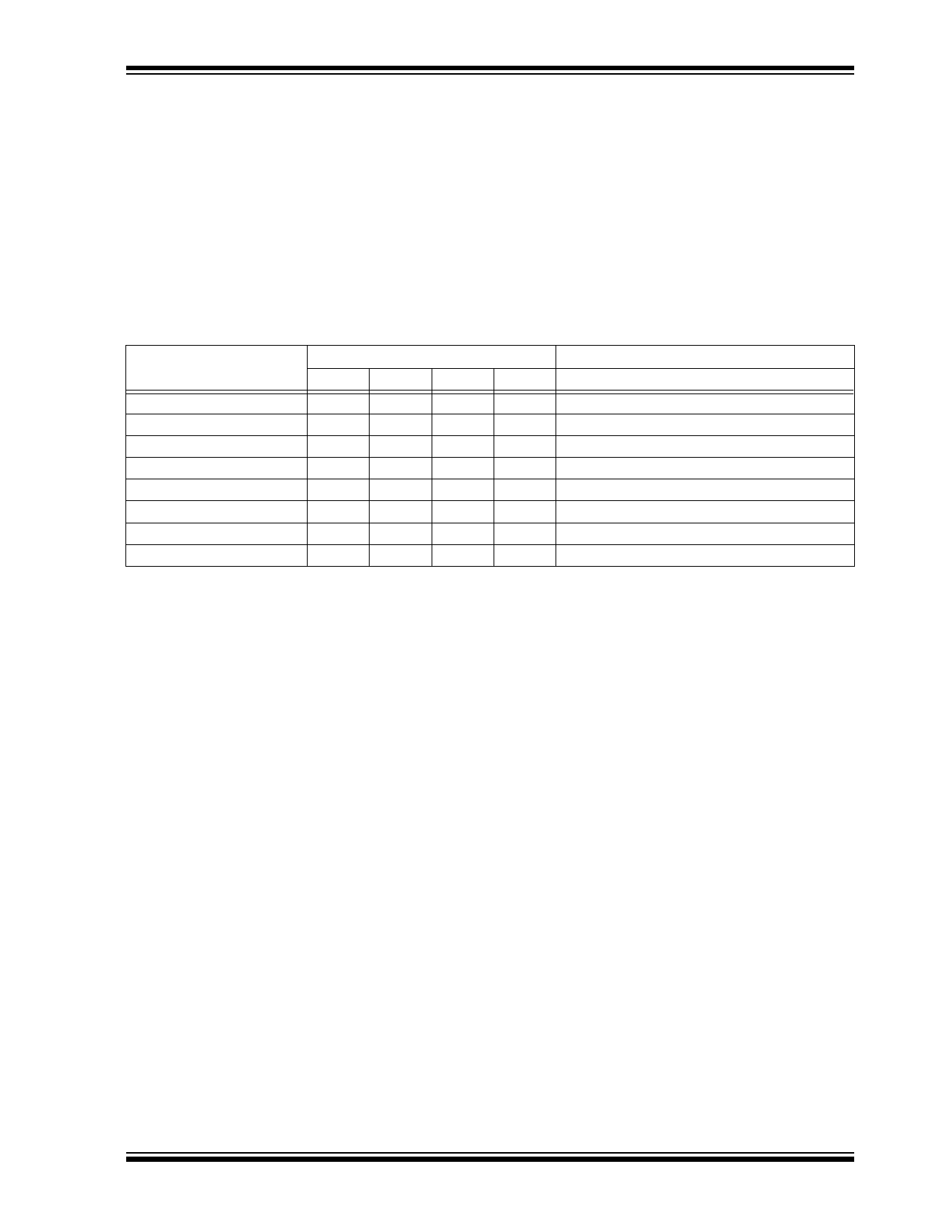
TABLE 4-3: SOFTWARE STATUS REGISTER BLOCK PROTECTION FOR SST25VF016B1
Status Register Bit2
Protected Memory Address
Protection Level
BP3 BP2 BP1 BP0
16 Mbit
None
X
0
0
0
None
Upper 1/32
X
0
0
1
1F0000H-1FFFFFH
Upper 1/16
X
0
1
0
1E0000H-1FFFFFH
Upper 1/8
X
0
1
1
1C0000H-1FFFFFH
Upper 1/4
X
1
0
0
180000H-1FFFFFH
Upper 1/2
X
1
0
1
100000H-1FFFFFH
All Blocks
X
1
1
0
000000H-1FFFFFH
All Blocks
X
1
1
1
000000H-1FFFFFH
1. X = Don’t Care (RESERVED) default is “0
2. Default at power-up for BP2, BP1, and BP0 is ‘111’. (All Blocks Protected)
2015 Microchip Technology Inc.
Downloaded from: http://www.datasheetcatalog.com/
DS20005044C-page 7
Share Link: 